In this article, we summarize their insights on the main trends, challenges, and possible solutions for the semiconductor industry in the coming years.
More and More Data
There are many driving factors for using semiconductors - cloud computing, 5G, Internet of Things, automobiles, mobile, AR/VR, mobile phones, etc. - just last year, as well as generating artificial intelligence and ChatGBT.
It is widely believed that by 2030, the semiconductor market will reach $1 trillion, almost twice the current level. In order to achieve this goal, billions of dollars in incentive measures have been established with the promotion of governments in the United States (CHIPS Act), Europe, Japan, South Korea, and China. Last year, it was also announced that billions of dollars would be invested in new factories and research centers. Efforts are currently being made to provide the required labor force.
One of the most useful ways to understand semiconductor demand is the amount of data generated, which of course must be collected, analyzed, and acted upon. "The amount of data generated every year is exploding," said Jaihyuk Song, corporate president and chief technology officer of Samsung Electronics' Device Solutions Business Unit. "It is more than two and a half times the number of stars currently estimated by space scientists in the entire universe."
Figure 1 illustrates this trend.
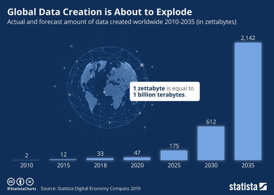
Figure 1
AMD Executive Vice President and CTO Matk Papermaster noted that if we keep the same pace, the power required for supercomputer installations will approach that of a nuclear power plant (Figure 2). "This is a very scary data point, and what it really tells you is that we are reaching the absolute limits of energy consumption," he said.
To this end, he proposed a new solution: changing computing methods, bringing memory closer to the CPU, and new more energy-efficient chip designs and architectures. “There will be a holistic approach to bending the curve to be able to improve our energy efficiency,” Pa permaster said. "We have to expand collaboration and more co-design optimization across the stack...and really drive system-level implementation. We have to think differently and really leverage innovation. If you look at what we've been doing The way things are designed — focusing on silos and then putting the pieces together — that doesn’t bend the curve at all,” he said.
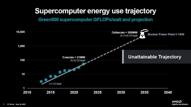
Figure 2
Artificial intelligence is bound to make the problem worse. “AI has large language models and the energy required for training will actually increase the speed and speed of energy consumption,” Papermaster said. He noted that billions of parameters are used today to train models such as ChatGBT3, but it is now being Toward Trillions of Parameters. "
The explosion of artificial intelligence
Imec CEO Van den Hove said that the rapid growth of generative artificial intelligence is driven by the following three main factors: the advancement of artificial intelligence models, access to large amounts of data, and substantial improvements in computing power. "The computational demands of AI are really exploding, and we're just getting started," he said. "To generate the required computing power in a sustainable manner, we will need devices and systems with substantially improved performance."Nvidia’s Jensen Huang also pointed out that the scale of deep learning has increased one million times in the past ten years. "Then, ChatGPT came along ... artificial intelligence spread across the world," he said. "ChatGPT is a generative pre-trained Transformer, a large language model with hundreds of billions of parameters, trained on trillions of words and sentences. It has learned the representation of human language and can generate text. ChatGPT is It's revolutionary for its ease of use and incredible functionality. It's a glimpse into the future of computers that can understand any programming language and perform a wide range of tasks."
Huang further pointed out that there are already more than a thousand generative artificial intelligence startups inventing new applications. For example, Tabnine is a contextual code assistant that can help complete lines of code or generate entire functions based on prompt descriptions. It can be programmed in a variety of popular languages, from JavaScript and Python to Rust, GO, and BASH.
Runway uses generative artificial intelligence to create and edit images and videos. The production quality was so impressive that it was used in several Oscar-nominated films. With Runway’s generative AI, anyone can tell stories through images and videos.
Insilico Medicine uses generative artificial intelligence technology to create a drug candidate in just one-third of the time at a time and at one-tenth the cost of traditional methods that typically take more than four years , costing approximately $500 million. Insilico Medicine is used by more than 20 pharmaceutical companies.
“The market impact of perception artificial intelligence is already huge,” Huang said. "The impact of generative AI will be even greater. Superior ease of use has enabled ChatGPT to reach over 100 million users in just a few months, making it the fastest-growing application in history." He said, Generative AI will be able to understand and enhance all forms of information, “from human language, music, pictures, videos and 3D to genes, proteins and chemicals”. He further supported that content on 200 million websites will be personalized and generated by AI, and billions of customer service calls will be automated by AI. Generative AI will also help 25 million software developers and hundreds of millions of creators.
What is the next wave of artificial intelligence? In Huang Renxun's view, the answer is "Embodied AI", which refers to intelligent systems that can understand, reason and interact with the physical world. Examples include robots, self-driving cars, and even chatbots that become smarter because they understand the physical world.
Cars make more demands
Automotive applications are another hot driver of semiconductor technology, including electric vehicles (EVs) and autonomous driving. In addition to advanced battery management systems, future vehicles will require next-generation sensing technology, combining multiple multispectral cameras and multiple radars, including short- and long-range radars. "All these sensors generate an incredible amount of data," Van den hove said. "To handle this, our cars will require entirely new computing architectures, running massive amounts of artificial intelligence on powerful centralized electronic control units. When evolving from current ADA systems to ever-increasing levels of autonomous driving, the computing required Capabilities are growing exponentially. Electronic control units in cars are actually rapidly advancing to what were once supercomputer performance levels," he said.He added that while the semiconductor content in cars will increase significantly, leading to growing demand for semiconductors, the total number of cars produced globally will not increase significantly. "It's really not obvious to design these extremely expensive computing systems on a chip and optimize them in a flexible way for specific markets like high-end and low-end markets," he said. "Therefore, we need to optimize these computing architectures taking into account flexibility, complexity, energy efficiency and affordability."
One approach that is generating interest in this regard is chiplet-based design, where the design is broken down into smaller silicon chiplets that are fused together using advanced heterogeneous integration techniques. "Using chiplets, ECUs can be configured in a more flexible way, allowing high-end or low-end configurations without having to redesign the entire chip. Since the chip will be smaller, it will allow IP to be reused, and it will provide better yield and reliability , which is crucial for the automotive industry," said Van den hove.
Moore's Law, 2D scaling, 3D stacking and chiplets
For decades, the semiconductor industry has enjoyed the benefits of the two-dimensional scaling defined by Moore's Law. As this type of scaling slows, alternative approaches such as chip stacking and chiplets are coming into play. "We believe that Moore's Law in the traditional sense remains critical. In fact, feature-based scaling by reducing the size of individual transistors remains one of the only technologies capable of delivering truly exponential growth in complexity." Van den hove Said.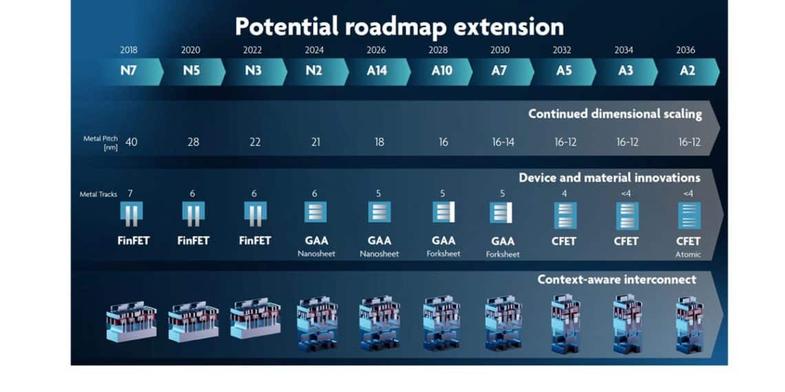
He presented imec’s roadmap for the next ten years (Figure 3), which includes continued use of 2D scaling as well as new technologies such as forksheet transistors and complementary FETs (CFETs). In the CFET architecture, n- and pMOS devices are stacked on top of each other, further maximizing the effective channel width. “By combining lithography-based scaling and introducing new interconnect schemes, new materials and new device architectures such as CFET device technology, we can achieve continued scaling for many more generations,” said Van den hove.
He also spoke of "walls" that may be insurmountable. the power wall (where it becomes increasingly difficult to scale the power consumption of each transistor) and the memory wall (defined by the delay between the time the CPU needs data from an SRAM-based cache or DRAM and the time it can access the data). “Because of the heavy workloads of AI, it is becoming increasingly difficult to efficiently transfer data to and from our processors.
In fact, for certain AI workloads in high-performance computers, in some cases the processors are active less than 3% of the time," he said. "Most of the time they are actually waiting for data. , so we need to rethink the memory system architecture. "
Imec also identified three additional walls:
Scaling Wall: Scaling enabled by pure lithography is slowing down. This becomes increasingly difficult as the individual structures of microchips and transistors are approaching atomic size and quantum effects begin to interfere with the operation of microchips.
Sustainability Wall: Manufacturing of semiconductor devices increases the environmental footprint, including greenhouse gases and water, natural resource and electricity consumption.
Cost wall: Clearly, as complexity increases, chip manufacturing costs, as well as design and process development costs, are likely to explode.
Van den hove said the industry will need a broad mix of technology options to achieve specific technology combinations to meet specific workloads and system requirements. "Interposer chips and tiny silicon bridge interposers will allow very fast connections between multiple core processor chiplets and 3D DRAM memory," he said.
Van den hove said the industry will need a broad mix of technology options to achieve specific technology combinations to meet specific workloads and system requirements. "Interposer chips and tiny silicon bridge interposers will allow very fast connections between multi-core processor chiplets and 3D DRAM memory," he said.
Today, DRAM memory is typically built as a stack of 3D layers, while the core processor chiplet is fabricated using a single chip (monolithic 2D system-on-a-chip). "The next approach to heterogeneous integration is to build advanced 2D processor chips as stacks of 3D layers, dividing functionality into layers. This can be done using advanced wafer stacking techniques, for example using through-silicon via technology , copper-to-copper hybrid bonding, enabling very high-density interconnects between the logic layer and the memory cache layer,” Van den hove said. Figure 4 illustrates how this looks in practice.
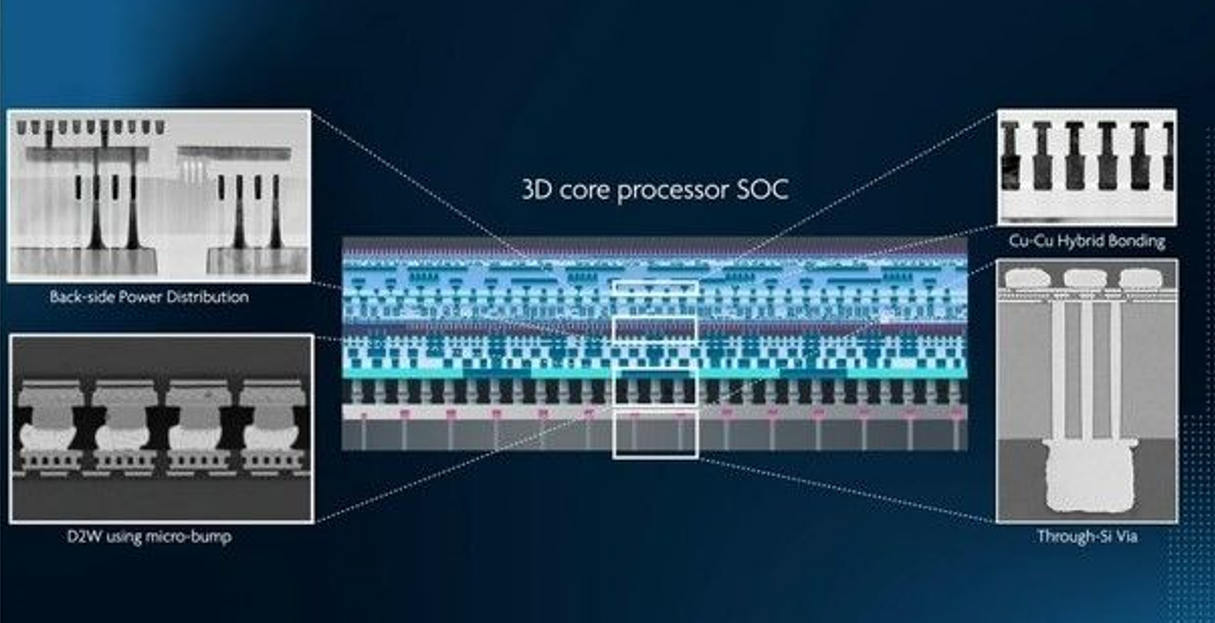
Figure 4
"We believe this will be one of the ways to extend Moore's Law even further than we thought was possible. We call this roadmap CMOS2.0, enabling further 2D scaling through the use of 3D stacking, enabling the next step in Moore's Law. stages. 3D alone gives us a linear increase in complexity," says Van den hove.
Another problem is that the power consumption of advanced chips is increasing so much that there are some constraints on extracting heat from the chip. "It is clear that in order to achieve such a complex 2D, 3D stacked core processor architecture, we need to solve the heating problem and learn how to cool the chip more efficiently. To do this, we are developing innovative cooling systems that can use 3D printing technology to manufacture,” said Van den hove. This direct liquid jet impingement cooling enables higher heat removal efficiency, five times higher than current state-of-the-art technology.
Samsung's Song pointed to trends particularly relevant to logic, DRAM and NAND device structures. In terms of logic products, in order to solve the problem of cell height scaling, he said that Samsung is developing backside interconnects. “Additionally, innovations in structure and materials, such as channel materials with optimal layer thickness, can enable excellent gate controllability compared to silicon channels,” he said (see Figure 5).
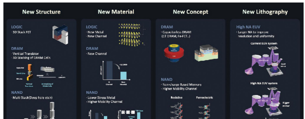
Figure 5
In DRAM, in order to solve the horizontal scaling problem, Samsung is working on a 3D structure in which vertical channels are stacked, which Song said is very different from the existing 2D structure. "We are also trying to introduce all low-leakage current channel materials, rather than the leakage-current controlled silicon channels that have been used so far," he said. "To address the cell capacitor issue, we are overcoming these limitations by investigating new concepts of capacitor-less DRAM."
On the NAND side, technologies such as multi-stack will continue to evolve. "New materials are needed to overcome mechanical stress or sensing margins. To further shrink unit device size, new concepts for device development that can lower the operating voltage are needed." "To improve the resolution and uniformity of EUV, larger mirrors are also needed high numerical aperture EUV technology."
The need for innovation and collaboration
"To continue to evolve in the digital transformation era, technologies to store and process such big data need new-age developments, and the semiconductor industry needs continuous innovation to make this possible," Song said.AMD's Papermaster points out that just a decade ago, deep neural networks began to show promise in accelerating computing. "There's no doubt we're still in the earliest stages," he said. "But I'm very hopeful because I know that if we get the right policies and the right restrictions, we're going to see this transformation over the next few years that will make us an incredible and productive city. We'll take advantage of AI-driven computing to accelerate innovation."
Van den hove says this requires "moonshot" thinking. “This will require collaboration across the value chain and across continents to skyrocket, bringing together the best minds. Like the missions to the moon in the sixties, we face seemingly insurmountable challenges. We must unite again to build A rocket fueled by innovation. But now we're not just aiming for the moon, we're aiming for a better planet, better life on Earth."