The development of the semiconductor industry is inseparable from industry consensus, and industry consensus is often reflected in the roadmap recognized by the industry. At the end of the last century, the American Semiconductor Industry Association SIA, in conjunction with the European and Asian semiconductor industries, began to publish the famous International Semiconductor Technology Roadmap (ITRS). The main contribution of ITRS is to coordinate the global semiconductor industry and publish chip technology roadmaps for more than ten years in the early 21st century, including feature size, power density, logic gate density, etc. By 2015, as the development of Moore's Law based on the traditional shrinkage of 2D CMOS feature sizes came to an end, ITRS was no longer updated, so the 2015 version was the last version of ITRS. At that time, as one of the leaders of ITRS, SIA issued a statement that it would release a new semiconductor roadmap at an appropriate time in the future. Last week, SIA and SRC jointly released a microelectronics and advanced packaging roadmap as the successor to ITRS.
Metrans is verified distributor by manufacture and have more than 30000 kinds of electronic components in stock, we guarantee that we are sale only New and Original!
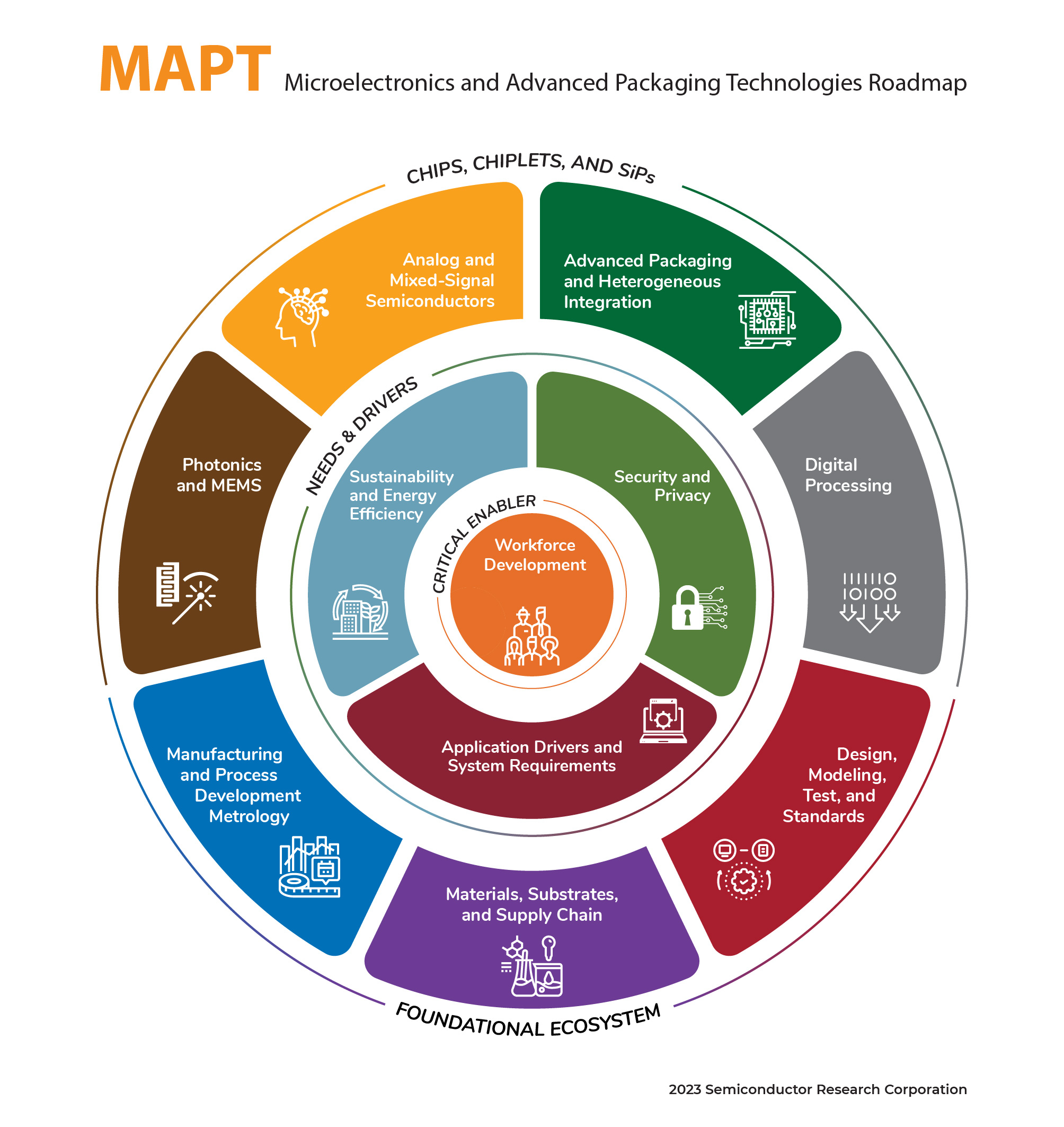
The MAPT roadmap is mainly aimed at the time range of the next ten years or so (2023-2035). It first analyzes the application requirements for the chip industry within the time range, including main driver applications, energy efficiency ratio requirements, and security requirements. Based on these requirements, it analyzes respectively It provides the corresponding technologies needed by various sub-sectors of the semiconductor industry (digital processing, advanced packaging and heterogeneous inheritance, analog and mixed-signal semiconductors, silicon photonics technology and MEMS, semiconductor processes, design modeling and test standards, semiconductor materials, and supply chain) progress to meet these needs.
First, the MAPT roadmap analyzes the most important driving applications expected for the semiconductor industry in the next ten years. The most important ones include:
- Data Center and High Performance Computing
- Vehicle electronics
- IoT and edge computing
- Mobile communications
- Biocomputing
In the MAPT roadmap, the main bottlenecks, required expertise and the most critical indicators of different driver applications are listed. From the analysis, we can see that computing and storage bottlenecks will become the most critical bottlenecks in future driver applications. In addition, interconnect bandwidth has also become a bottleneck in several important driver applications. In terms of core indicators, the most critical indicators Basically they all point to performance and power consumption. Therefore, from the perspective of driver applications, the direction of progress of the semiconductor chip industry in the next decade or so is very clear: by further improving computing, memory and data interconnection performance to meet the needs of several important driver applications, and at the same time by optimizing design. requirements for power consumption. Since performance and power consumption are both important at the same time, the indicator of energy efficiency ratio is expected to become the most critical indicator in the field of semiconductor chips in the next ten years - in fact, in the MAPT roadmap, the word "energy efficiency ratio" is repeated Nearly 120 times, which shows its importance.
Digital chips: Logic density growth slows down, architectural innovation drives technological progress
Digital chips have always been the core category of semiconductor chips. They have large shipments and are highly dependent on semiconductor chip technology. They are often the core chip category that drives the development of the entire semiconductor industry. Therefore, in the MAPT roadmap, for digital chips The relevant roadmap analysis is also the most detailed.
In the roadmap for digital chips, we first saw numbers that were completely different from those predicted by Moore's Law. The MAPT roadmap predicts that in the next ten years, transistor density will increase from the current 20 billion per square centimeter to 80 billion per square centimeter, which is a fourfold increase in 10 years. In the past, Moore's Law predicted that transistor density would double every 18 months, so transistor density should increase by more than 64 times in 10 years. From this point of view, according to MAPT's roadmap, the growth rate of transistor density in the future will be much lower than that of previous Moore's Law. The rate of increase in transistor density in the next ten years is only equivalent to the level of the past three years.
And if we look carefully at the evolution of semiconductor processes in recent years, we can find that in fact the improvement in transistor performance (i.e. gate delay) lags behind the previous prediction of Moore's Law of 40% improvement every 18 months - currently every While the integration level of the next generation process has doubled, the transistor performance has only improved by 10-20%, and this number will be even smaller in the future. Therefore, from the MAPT roadmap, we can roughly estimate that in the next ten years, as the level of transistor integration quadruples, the performance of transistors will increase by about 20-30%. In other words, digital chip performance improvement cannot basically rely on transistor performance improvement, but must rely on other methods.
In MAPT, the future progress of digital logic mainly depends on architectural progress. MAPT proposes that the main directions for progress include:
- Further improve integration: Since semiconductor process advances will have limited contribution to the improvement of logic density in the next decade, in order to further improve integration, we mainly need to rely on advanced packaging technology. Advanced packaging technology can use different stacking methods (2.5D and 3D) to integrate different chiplets into the same package and can solve the yield problem of advanced processes. Therefore, it is expected to be more popular in mid-to-high-end chips in the future. Wide range of applications.
- Reduce data movement overhead: As chips become more integrated in the future (i.e., the logic becomes more complex), the overhead of data interconnection will become the main bottleneck in chip performance and energy efficiency ratio; for example, according to previous research, at the 10nm node , the power consumption of data interconnection in highly complex SoCs has accounted for about 90% of the entire chip power consumption. In the future, as the complexity and integration level further increase, data interconnection will increasingly become a bottleneck. In order to solve this problem, on the one hand, advanced packaging technology needs to be used - for example, through 3D stacking, the physical distance of the interconnection will be greatly reduced (because it can be routed vertically), thereby reducing power consumption; another focus is through new architecture, For example, near-memory computing and in-memory computing can reduce overhead; finally, innovations in analog and mixed-signal circuits can also reduce data movement overhead.
- Using more domain-specific design architectures instead of general-purpose designs - such as using AI accelerators to perform artificial intelligence-related calculations (rather than using general-purpose architectures such as CPUs and conventional GPUs) - can greatly improve energy efficiency. . When using a purpose-designed architecture, software and hardware co-design will become a core concept, because when designing a purpose-built architecture, the actual needs of the software and application layers need to be considered (for example, for AI accelerators, it is a dedicated number system and specific algorithm). character support), thereby achieving high efficiency. In addition, when using a dedicated architecture, chip technology can be used to implement different architectures using multiple chip particles and integrate them using advanced packaging technology.
Advanced packaging technology: Rapid technology evolution has become the backbone of the industry
As MAPT analyzes in the digital logic chapter, advanced packaging will become the main theme of future semiconductors.
For example, in the next five years, the number of chip dies in a system will increase from 4-10 today to 10-30 (an increase of 3 times). It is expected that the number of chip dies will increase even more within ten years; in memory From a perspective, chip chips will implement a new memory architecture, thereby improving the memory wall problem. By then, it is hoped that the capacity, speed and power consumption of the memory will no longer become the bottleneck of the entire system; in terms of interconnection, the interconnection lines of advanced packaging in the next 10 years The number will increase from today's 1000-2000 to 8000, and new IO interface technologies (such as PAM8, and high-density WDM optical interconnect) will be used to further increase data bandwidth and reduce data movement overhead.
These requirements specifically correspond to the technological evolution of advanced packaging. MAPT proposes the direction of technology evolution in the next ten years in the advanced packaging chapter.
We believe that the most critical technology evolutions in advanced packaging over the next decade include:
- Further improve IO density: reduce the bump (solder ball) distance between chip particles from 100 microns to 25 microns, thereby increasing IO density by 16 times.
- Further improve the IO interconnect line density: The interconnect line density here includes developing today’s 2-3 top-level copper interconnects with line spacing greater than 1 micron on the front side of the wafer to 7 layers of copper interconnection with line spacing less than 1 micron, and on the back of the wafer. The RDL layer interconnection is raised from one layer to three layers of interconnection and the line spacing is reduced from 10 microns to 2 microns; and the interconnection line spacing between wafers is reduced from 5 microns to 1 micron, which means the interconnection line density is increased by 25 times.
- Innovative integrated bonding technology: From the current solder-based bonding integration technology to gradually improved to die-to-wafer and die-to-die bonding. New integrated bonding technology will be the core technology to achieve high-density IO.
Analog and Mixed Signal: The Heart of Wireless Communications and Power Electronics
Analog and mixed-signal circuits also play an important role in the semiconductor roadmap for the next decade, as analog and mixed-signal circuits will continue to be an enabling technology for important applications.
The first core application of analog and mixed-signal circuits is wireless communications. It is expected that in the next 10 years, the demand for data rates in wireless communications will continue to rise. In order to support higher data rates, higher bandwidths need to be used at higher carrier frequencies, and circuit performance (linearity, noise coefficients, etc.) continue to evolve.
Specific to the wireless communication analog mixed-signal circuit roadmap, we can see the evolution of some core indicators:
- The carrier frequency has evolved from less than 40GHz today to 175GHz, while the bandwidth has increased from 100MHz today to 5GHz.
- The low-noise amplifier coefficient remains near 4 dB, but the operating frequency increases from the maximum supported 90GHz to 250 GHz
- The efficiency of the power amplifier remains at 30%, but the supported frequency increases from 90GHz to 250GHz
- The complexity of the antenna array has been greatly increased, from the current 64 elements to 1024 elements
In the roadmap, we can see that both GaN and SiC power electronic chips will make great progress. For SiC, it is expected that in the next 10-15 years, the supported voltage will expand from today's 3.3kV to 15-25kV, thereby providing support for new energy applications, while also further increasing the device carrier movement rate to improve device performance. (Supporting higher switching frequencies); GaN is also providing high device performance and switching frequencies while increasing support for high voltages, from today's 650V to 3.3kV. In addition, another important evolution direction is To further improve GaN’s support for silicon substrates (GaN on Silicon), it is expected that 200mm GaN-on-silicon wafers will become standard configuration in 10 years, thereby further reducing the cost of GaN and having the opportunity to support more convenient advanced packaging integration.