On December 6, Google officially announced the new multi-modal large model Gemini, which includes three versions. According to Google's benchmark test results, the Gemini Ultra version has shown "the most advanced performance in many tests”, even completely beating OpenAI’s GPT-4 in most tests.
Metrans is verified distributor by manufacture and have more than 30000 kinds of electronic components in stock, we guarantee that we are sale only New and Original!
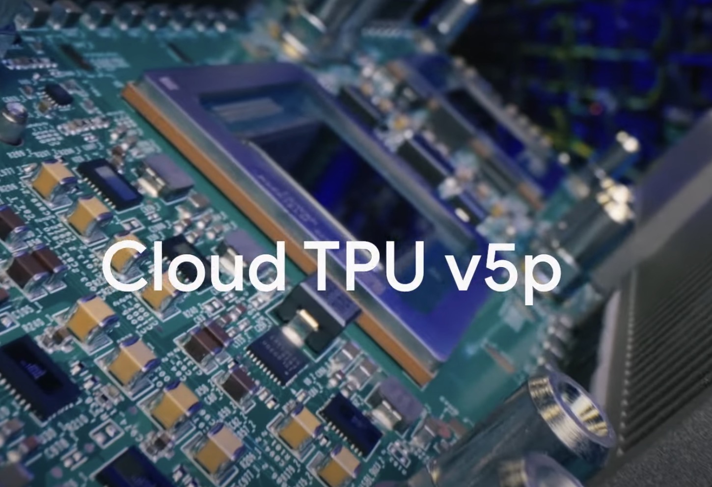
While Gemini stole the show, Google also dropped another blockbuster - the new self-developed chip TPU v5p, which is also the most powerful TPU to date.
According to official data, each TPU v5p pod combines 8,960 chips at a speed of 4,800 Gbps/chip through the highest bandwidth inter-chip interconnect (ICI) in a three-dimensional ring topology. Compared with TPU v4, TPU v5p's FLOPS and high-bandwidth memory (HBM) are increased by 2x and 3x respectively.
In addition, TPU v5p trains large LLM models 2.8 times faster than the previous generation TPU v4, and with second-generation SparseCores, TPU v5p trains embedding dense models 1.9 times faster than TPU v4. TPU v5p is also 4x more scalable than TPU v4 in terms of total available FLOPs per pod, with twice the number of floating point operations per second (FLOPS) and twice the number of chips in a single pod , greatly improving the relative performance of training speed.
Google also hired a bunch of scientists to endorse the AI performance of TPU v5p:
Erik Nijkamp, senior research scientist at Salesforce, said: "We have been leveraging Google Cloud TPU v5p to pre-train basic Salesforce models that will serve as the core engine for professional production use cases, and we have seen significant improvements in training speed. In fact, Cloud TPU v5p offers up to 2x the compute power of the previous generation TPU v4. We also really like the seamless and easy transition from Cloud TPU v4 to v5p using JAX. We are excited to have accurate INT8 training with the Accurate Quantization Training (AQT) library formats to optimize our models, further increasing speed.”
Dr. Yoav HaCohen, head of the core generative AI research team at Lightricks, said: “Leveraging the superior performance and ample memory of Google Cloud TPU v5p, we successfully trained a text-to-video generative model without the need to split it into separate processes. . This optimal hardware utilization greatly speeds up each training cycle, allowing us to quickly launch a series of experiments. The ability to quickly train the model in each experiment promotes rapid iteration, which is what our research team is competing for a valuable advantage in the field of generative artificial intelligence."
Jeff Dean, chief scientist of Google DeepMind and Google Research, also supports his own chips: “In early use, Google DeepMind and Google Research observed that the speed of LLM training workloads using TPU v5p chips was increased by 2 times compared with the TPU v4 generation. Strong support for ML frameworks (JAX, PyTorch, TensorFlow) and orchestration tools allow us to scale more efficiently on v5p. With the second generation of SparseCores, we also see significant performance improvements for embedded workloads. TPU for It's critical that we do the largest research and engineering work possible on cutting-edge models like Gemini."
For Google, Gemini is a powerful tool to deal with Open AI, and TPU v5p is a stepping stone. Use it to build a high wall against NVIDIA GPUs. With both software and hardware, it seems that it is already in a bad position in the AI era. The place of defeat.
Why does Google have the advantage it currently has?
From unknown to famous all over the world
Google TPU was not achieved overnight. Its self-research journey began ten years ago.
As a technology company, Google actually considered building an application-specific integrated circuit (ASIC) for neural networks as early as 2006, but by 2013, the situation became urgent. Google scientists began to realize that the rapid growth of neural networks There is an irreconcilable contradiction between computing needs and the number of data centers.
Jeff Dean, the head of Google AI at the time, calculated and found that if 100 million Android users used the mobile phone voice-to-text service for 3 minutes a day, the computing power consumed would be twice the total computing power of all Google data centers, and Android users around the world are far More than 100 million.
The scale of the data center cannot expand indefinitely, and Google cannot limit the time users use services. However, both CPU and GPU are difficult to meet Google's needs: the CPU can only handle a relatively small number of tasks at a time, and the GPU The efficiency is lower when performing a single task, and the range of tasks that can be handled is smaller. Self-research has become the last way out.
Google has set a small goal: to build a domain-specific computing architecture (Domain-specific Architecture) for the purpose of machine learning, and to reduce the total cost of ownership (TCO) of deep neural network inference to one-tenth of its original value.
Usually, the development of ASIC takes several years, but Google completed the design, verification, manufacturing and deployment of the TPU processor to the data center in only 15 months. Norm Jouppi, the technical lead of the TPU project (and one of the main architects of the MIPS processor), described the sprint phase this way:
"Our chip design is very fast. It's really remarkable. We started shipping the first chip without fixing bugs or changing masks. Considering we were building the chip while still hiring a team, then Hiring RTL (circuit design) people and rushing to hire design verification people, it's all very hectic."
The first-generation TPU, which represents the crystallization of Google's technology, is manufactured using a 28-nanometer process, with an operating frequency of 700MHz and a running power consumption of 40W. Google packages the processor into an external accelerator card and installs it in a SATA hard drive slot to achieve plug-and-play. use. The TPU connects to the host via the PCIe Gen3 x16 bus, providing an effective bandwidth of 12.5GB/s.
Compared with CPUs and GPUs, single-threaded TPUs do not have any complex microarchitectural features. Minimalism is the advantage of domain-specific processors. Google's TPU can only run one task at a time: neural network prediction, but the performance per watt is It has reached 30 times that of GPU and 80 times that of CPU.
Google was very low-key on this matter. It was not until the 2016 Google I/O Developer Conference that CEO Sundar Pichai officially showed the world the self-research results of TPU.
Pichai told the guests attending the meeting that AlphaGo developed by DeepMind was able to defeat Korean chess player Lee Sedol, and the TPU in the underlying hardware was indispensable. TPU is like Helen, the woman who triggered the Trojan War in Greek mythology. Its appearance caused "adult... Thousands of chips compete with it."
But Google did not stop there. Almost as soon as the first generation of TPU was completed, it immediately invested in the development of the next generation: in 2017, TPU v2 came out; in 2018, TPU v3 was launched; in 2021, TPU v4 was launched on Google I/O Appeared at Developer Conference…
And Google is becoming more and more comfortable with AI chips: the first-generation TPU only supports 8-bit integer operations, which means that it can perform reasoning, but training is out of reach; and TPU v2 not only introduces HBM memory, but also supports floating Point computing supports the training and inference of machine models; TPU v3 focuses on enhancing performance based on the previous generation, and quadruples the number of chips deployed in the Pod.
When it comes to TPU v4, Pichai proudly said: "The progress of AI technology depends on the support of computing infrastructure, and TPU is an important part of Google's computing infrastructure. The new generation TPU v4 chip is more than twice as fast as v3." Google uses TPU clusters to build Pod supercomputers. A single TPU v4 Pod contains 4096 v4 chips. The interconnection bandwidth between chips of each Pod is 10 times that of other interconnection technologies. Therefore, the computing power of a TPU v4 Pod can reach 1 ExaFLOPs, which perform 10 to the 18th power floating-point operations per second, are equivalent to the total computing power of 10 million laptops.”
Today in 2023, TPU has become one of the synonyms of AI chips and another important processor after CPU and GPU. It is deployed in dozens of Google data centers and completes hundreds of millions of tasks every day. AI computing tasks.
Google’s Self-research Empire
TPU is just the prelude to Google’s self-research.
At the Google Cloud Next '17 conference in 2017, Google launched a custom security chip called Titan, which is designed for hardware-level cloud security and enables more secure identification and authentication by establishing an encrypted identity for specific hardware. This prevents increasingly rampant BIOS attacks.
The Titan chip is not all for Google itself. It appears to convince enterprises that data stored in Google Cloud is more secure than the enterprise's local data center. Google said that the self-developed Titan chip establishes a strong hardware-based system identity. To verify system firmware and software components and protect the startup process, all this benefits from the hardware logic created by Google itself, which fundamentally reduces the possibility of hardware backdoors. The Titan-based ecosystem also ensures that facilities only use authorized and accessible The verified code ultimately allows Google Cloud to be more secure and reliable than on-premises data centers.
The emergence of Titan is just a small test. In March 2021, Google introduced a self-developed chip for YouTube servers for the first time at the ASPLOS conference, namely Argos VCU. Its task is very simple, which is to process the videos uploaded by users. Transcode.
According to statistics, users upload more than 500 hours of video content in various formats to YouTube every minute, and Google needs to quickly convert this content into multiple resolutions (including 144p, 240p, 360p, 480p, 720p, 1080p, 1440p, 2160p and 4320p) and various formats (such as H.264, VP9 or AV1). Without a chip with powerful encoding capabilities, it is impossible to quickly transcode.
Google has tried two solutions. The first is Intel's Visual Computing Accelerator (VCA), which contains three Xeon E3 CPUs with built-in Iris Pro P6300/P580GT4e integrated graphics core and advanced hardware encoder. The second one uses Intel Xeon processors plus software coding to get the job done.
But both the former and the latter require huge server scale and huge power consumption. Therefore, Google started the research and development of another self-developed chip-VCU. Starting in 2015, a team of about 100 Google engineers worked on designing the first generation of Argos chips, said Scott Silver, Google's vice president of engineering who oversees YouTube's vast infrastructure. Among them, this team not only completed the research and development, but also applied the chip in Google's data center, and the strength of Argos was also demonstrated - it processes video 20 to 33 times more efficiently than traditional servers, processing high-resolution 4K video time was shortened from days to hours.
The next generation of Argos may have already been quietly launched on Google servers. According to reports, Google’s self-developed second-generation VCU will support AV1, H.264 and VP9 codecs, which can further improve the efficiency of its encoding technology and will also be The most powerful support for YouTube content creation ecology.
And Google’s strongest move is the most complex mobile phone SoC. On October 19, 2021, at an autumn conference, the flagship phone Pixel 6 series equipped with Google’s first self-developed chip Tensor made its debut.
Google Senior Vice President Rick Osterloh said at the press conference that this chip is "the largest mobile hardware innovation in the company's history." Google CEO Sundar Pichai even posted a photo of the Tensor chip on Twitter early. The pride in the research project is palpable.
However, this self-developed chip is essentially based on the semi-custom chip design service opened by Samsung in 2020. In the disassembly diagram of TechInsights, the package size of Tensor is 10.38mm x 10.43mm = 108.26mm 2, and the internal chip logo It is "S5P9845", which conforms to the traditional Samsung Exynos processor naming rules. For example, the Exynos 990 chip is marked as S5E9830, and the Exynos 2100 5G SoC chip is marked as S5E9840. It is essentially a chip defined by Google and designed and manufactured by Samsung.
Even so, the layout of Google's self-developed chips has begun to take shape. From TPU to Titan, from VCU to Tensor, Google has gone through a ten-year journey, and its ambition to fully master this empire of silicon chips is also clear. Reveal.
Google's Stumbling Block
For Google, it needs money, technology and technology, and application scenarios. It can be said that among the major technology giants, it has gone the furthest on the road of self-developed AI chips. Other manufacturers are still continuing to do so. Google is constantly adding money to Nvidia's account, but Google has already made preparations for both. Many people even regard it as the strongest challenger to Nvidia's monopoly today.
Compared with Microsoft and Amazon, Google's most prominent advantage is to design TPU from a system-level perspective. A single chip is important, but how it is used in combination in the system in the real world is even more important. Although Nvidia also thinks from a systems perspective, their systems are smaller and narrower in scope than Google. And Google also uses a custom network stack ICI between TPUs. This link offers low latency and high performance compared to expensive Ethernet and InfiniBand deployments, similar to Nvidia's NVLink.
In fact, Google's TPUv2 can scale to 256 TPU chips, the same number as Nvidia's H100 GPU. In TPU v3 and TPU v4, this number increases to 1024 and 4096 respectively. According to Trendline, the latest TPU v5p can scale to 8960 chips without going through inefficient Ethernet.
In addition, Google also has unique advantages in OCS, topology, and DLRM optimization. The experience and advantages accumulated over the past ten years have helped Google’s TPU to show its talents in data centers and AI large models. In specific applications, it is far ahead. It’s not an exaggeration to describe it. It’s not impossible for Google to completely get rid of the constraints of NVIDIA GPUs in the future.
However, Google still has a minor stumbling block.
The self-research of TPU started in 2013, and it was able to be quickly deployed to the data center within 15 months, and at the same time achieve a rapid iteration performance increase. In addition to Google researchers working around the clock, the help provided by another company was also extremely important.
According to a report by J.P. Morgan analyst Harlan Suhr in 2020, the generations of Google TPU v1 to v4 were co-designed by Broadcom. At that time, it had begun producing TPU v4 using the 7nm process and began to cooperate with Google in designing and adopting TPU v5 with 5nm process
Sur said that Broadcom's application-specific integrated circuit (ASIC) business had revenue of US$750 million in 2020, up from US$50 million in 2016. In addition to chip design, Broadcom also provides Google with key intellectual property and is responsible for In addition to steps such as manufacturing, testing and packaging new chips to supply Google's new data centers, Broadcom is also working with other customers such as Facebook, Microsoft and AT&T to design ASIC chips.
According to Broadcom's 2022 financial report, it divides ASIC revenue into two parts: routing and switching and computing offloading. Compute offloading is handled in the data center in two steps. When a compute request comes in, routers and switches decide which part of the data center should handle the work. Once decided, a processor (usually a CPU or GPU, like those designed by Nvidia) does the calculations, which are then sent back to the end user by those routers and switches again over the Internet or private network.
Broadcom is the world's second-largest artificial intelligence chip company in terms of revenue, behind Nvidia, and its ASIC sales amount to billions of dollars, which is the result of Google's increased TPU deployment in response to Microsoft's cooperation with OpenAI. , just one Google TPU has more than quadrupled Broadcom's ASIC revenue. The artificial intelligence tax that Google did not pay to Nvidia went into Broadcom's pocket in another form.
No matter which company it is, it will not be willing to continue to pay this money. Therefore, in September this year, it was reported that Google was preparing to end its partnership with Broadcom before 2027. Sources said that Google executives have set a Abandoning Broadcom's goal, it began to consider its rival Marvell after the two companies were locked in a months-long impasse over the pricing of TPU chips.
Although Google officials later came out to refute the rumors, saying that there are currently no plans to change the cooperative relationship with Broadcom, it is already known that the two companies are at odds in private.
Google made a smart calculation on TPU. When giants such as Microsoft paid obediently, it took out TPU v5p to fight against Nvidia. But what it did not expect was that ASIC cooperation, which was inconspicuous a few years ago, is now It has become the biggest stumbling block on the road to TPU development. As long as the deployment scale of TPU is expanded, Broadcom will have to continue to add money.
Thinking about it this way, the giants can really escape the first grade of junior high school, but they can't escape the fifteenth grade. They can escape the 70% profit of Nvidia GPU, but they can't escape partner companies like Broadcom and Microsoft. They want to develop AI chips. Save money, you will inevitably encounter difficulties like Google today in the future.