
Metrans is verified distributor by manufacture and have more than 30000 kinds of electronic components in stock, we guarantee that we are sale only New and Original!
A lot has changed over the past few process nodes. A growing number of startups are successfully building advanced-node chips at costs well below those highly cited figures. Behind those numbers are some broad changes in chip design and manufacturing. These include:
- Many advanced node chips are either highly replicated arrays of multiple cumulative processing elements for AI/ML. These components are relatively simple compared to integrating different components on a single chip, but they need to be characterized for thermal issues, noise, and various use cases and applications.
- Advanced packaging technology has become mainstream since these early estimates, allowing chipmakers to bundle together chips or chipsets developed at different process nodes rather than trying to push analog capabilities to 5nm or higher. node, this is both expensive and unhelpful.
- In the past, adopting the latest nodes ensured market leadership in performance and power consumption. This is no longer the case. Improvements in mature nodes, as well as architectural changes involving hardware and software, allow many chipmakers to delay migration to the latest nodes, at least until these processes have matured to the point where they are cost-effective.
For example, many believe that all new chips will fill a grille and that designs will continue to grow in size and complexity. In some cases, complexity does increase - well beyond the point where all the latest features can be achieved on a single reticulated tube - but many of these new features are a mix of the latest process geometries and established process nodes. developing. In other cases, the number of processed components in a package increases, but the complexity actually decreases.
Software is another deciding factor. Not all software needs to be developed from scratch. Additionally, there are a wealth of tools and ecosystems readily available for Arm, NVIDIA, and a growing number of RISC-V designs. Nearly all major EDA companies are investing heavily in AI/ML to shorten and improve the design process, particularly in software debugging, and to more effectively leverage expertise across the company through reinforcement learning.
Some Stark Numbers
Back in 2018, the last time anyone made such an estimate, IBS published the chart shown in Figure 1 . The chart puts the cost of a 5nm chip at $542.2 million. If this is true, then apparently only two-thirds of the chips are in production today, and probably no one is looking at chips beyond 3nm.
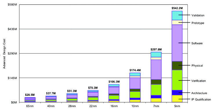
Soures:IBS 2018 IBS 2018
If we go back a few years and compare this to a chart produced by IBS in 2014 (see Figure 2), we can see how these estimates have changed over time.
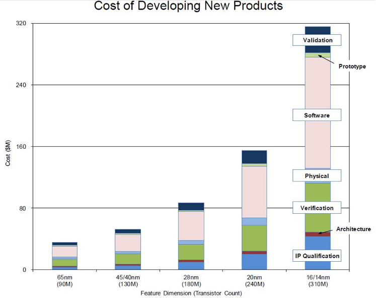
Soures:IBS 2014 IBS 2014
Note that the estimated cost of 16nm/14nm dropped from about $310 million to $106 million. Going back even further, 28nm dropped from about $85 million to $51 million. Whether this is an overshoot of estimated costs or reflects a sharp drop in costs as new nodes mature is open to debate. However, if the latest figures are converted into similar amounts, a 5-nanometer chip would cost around $280 million and a 7-nanometer chip would cost around $160 million.
"Think Qualcomm or Nvidia," said Isadore Katz, senior director of marketing and business development at Siemens Digital Industrial Software. Isadore Katz, senior marketing director at Siemens Digital Industrial Software, said: "If it really costs $542 million to make a new chip, then only they and a few other companies have the ability to do it. But they will not make the chip using 5 nanometers." They'll take an architecture, do some innovation on that architecture as part of the transition to a new process node, and then they'll develop a family of parts that run on that process node.
Few companies publish their actual costs, but you can find a rough idea by looking at the venture capital a company received to see how much money they burned when they released their first chip. "Innovium built the original chip for $150 million, and they later raised a new round of funding for $100 million to fund multiple generations of products," said Nick Iliadis, senior director of product planning at Achronix. Ilyadis) said. "Since its founding in 2014, Innovium has received a total of $402 million in funding across 10 rounds and will still have $145 million in cash on hand when it sells to Broadcom for $1 billion in 2021. Their third The first-generation chips are manufactured using a 7-nanometer process."
A large part of the cost is the first mover penalty. "The expenses associated with large digital chips have exploded," said Marc Swinnen, director of product marketing at Ansys. "That's where those big headline numbers come from. If you look at how long it takes Apple to create a new chip, that's 18 months, hundreds of designers, licenses, a whole new mask set and advanced processes. That's That's when costs go up. But if you can use older nodes, those costs are much lower now.
There may also be some costs hidden in these numbers. "Recharacterizing the functionality of new transistors, getting mask manufacturing capabilities in place, understanding manufacturing issues, and creating extraction models does require significant investment," said Siemens' Katz. "But we are leveraging the lessons learned from previous nodes, and once we have those building blocks, BSIM-CMG models, extraction models, die changes and metallization, we will be able to leverage parametric or process-independent techniques on top of that." .
These numbers make others curious. "This is a diagram I drew 12 years ago (see Figure 3)," said Frank Schirrmeister, vice president of solutions and business development at Arteris. "I received four or five sets of data from IBS but couldn't publish the numbers, so the chart I drew was an average of the spending categories. This shows the main steps in chip development. It shows along the x-axis from RTL development to Timeline of tape out. Then the percentage of the total project effort is shown on the Y-axis."
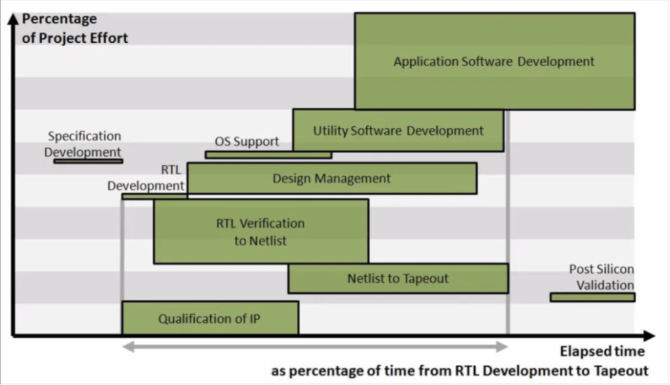
Source:Frank Schirrmeister Frank Schirrmeistersoures
Based on Figure 3, you can consider whether any of these may change over time, or as size or production nodes change. For example, it is often said that verification costs rise quadratically as chip size increases, but history shows otherwise. "Verification costs do go up because the larger the design, the longer it takes to simulate and the more test cases you have to generate," Ilyadis said. "You can take the previous generations of benchmarks and keep running them," Ilyadis said. "And then there are new tests related to the new features. That requires more servers, bigger servers, more disks. Those will As additional costs ripple through the infrastructure.
Is infrastructure included in published costs? "Understanding the details of these numbers is key," said Arteris' Schirrmeister. "Is all software included? How much new RTL development is included? How much verification is required? Do you need to buy an emulator? When you consider the cost of the mask, that touches at least an order of magnitude for these chips."
Some costs do come down over time. "When you think about the cost of IP, you either have to develop it (which requires using in-house engineering resources) or you have to license it (which means you pay a vendor)," Ilyadis said. "Typically, a license comes with support and maintenance, and that's a cash outlay," Iliadis said. "Then there's the cost of tooling. Each generation requires a new set of tools as routing becomes more complex or considerations need to be Many more factors. There's also the labor cost of the team that develops the chip. Plus you have to build test fixtures and even products to display the chip. Now, we've gotten beyond the chip itself, but all of this has to do with the actual chip development and About what it takes to bring a chip to market. Then, there's that gift that keeps coming - software. Most chips have some sort of programmability. Beyond that, there's manufacturing, including testers, test fixtures and burn-in fixtures for accelerated life testing.
Even the cost of IP can be an important variable, especially if one takes into account the time saved by purchasing the IP, or the indirect costs associated with developing the IP. "The increase in SoC design cost and complexity has put greater pressure on computing infrastructure," said Brian Jeff, senior director of product management for Arm's infrastructure business line. "This is driving the trend toward custom silicon to deliver specialized processing for specific workloads and achieve massive efficiencies," said Brian Jeff, senior director of product management for the Infrastructure business line at Arm. "By developing IP with a customizable foundation, IP Providers can take on many of the common integration, verification and validation tasks that partners have to iterate on design after design. In this way, partners can focus resources on those features that help them differentiate and design based on their workload out complete silicon. In one example, one partner reduced development costs for its high-end infrastructure SoC by 80 engineering years."
Many costs are incremental. "We don't relearn everything between process nodes," Katz said. "We remember what we have to do. We put a lot of effort into the parameterization or representation of the design artifacts, from the top-level test bench, the way we describe the IP, the way we articulate custom logic and accelerators, all the way down to how we lay out the cells. . We learn what needs tweaking and make corrections with dials and knobs. We don’t start from scratch between nodes. Even if we change the way the transistor surface works, or we reorganize the way the first layer of personalized metal works, We also need to spend extra time characterizing it. We need to spend more time understanding how to extract this characteristic, and we may need to make small and modest adjustments to our battery design to accommodate this characteristic. But The basic topology exists.
Well-developed IP can be reused across multiple chip generations. Companies like Intel, AMD, Marvell, Broadcom, Nvidia, and Qualcomm all develop significant amounts of IP in-house. Some of these come in the form of chips that can be fully characterized and reused in predetermined architectures. This comes at the expense of in-house expertise, but also reduces surprises on site, and there are no licensing costs.
EDA Cost
Each node creates new issues and challenges that often require EDA vendors to make significant investments in new tools or process creation. When new nodes emerge, many tools are rudimentary and solutions are patched together. I don’t know what technology can be used to solve the problem.
Over time, as the industry learns what works and what doesn’t, processes improve and eventually become automated. "Many challenges were overcome through brute force," says Ansys' Swinnen. "They leveraged existing tools and enough people to make it work. It requires close collaboration with suppliers. It's not a process that the average mainstream chip designer has mastered. As we learn from them over time, They also learn from us. The tools are getting better, the degree of automation is increasing, the rough edges have been smoothed out, and the manual steps in the middle have been reduced. This has made productivity significantly higher.
However, what works today may not work in the future. "You have to plan for a bunch of things," Katz said. "I've been involved in things like timing, process variations, and ground bounce. When you drop the voltage threshold below 1V, a lot of problems arise. That was unknown when we got to 14nm. Today, people understand that. . People understand the issues that can arise in the timing or layout of a design. They understand what they have to pay attention to in terms of the impact of metal on latency and timing, and they are becoming increasingly aware of some of the physical side effects, susceptibility to surge noise, Susceptibility to electrical leakage. These are the stuff of the playbook. This playbook will take you through every conundrum of the past 10 or 15 years. How to solve these problems? How to achieve automation? Or, how to design and solve these problems?
Figure 4 is another old chart worth revisiting. Andrew Kahng and Gary Smith in 2001 conducted an analysis of design costs to illustrate how new EDA developments affect productivity. This analysis was published by ITRS in 2002.
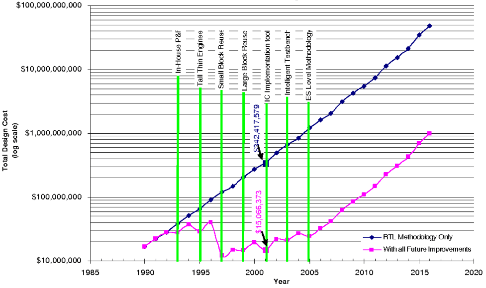
Source :"Proceedings of the 2002 International Symposium on High Quality Electronic Design": Proceedings of the 2002 International Symposium on High Quality Electronic Design
Although this indicates future technologies such as ESL that have never appeared before, other technologies have emerged. Subsequent publications by ITRS showed that development costs remained stable to some extent, with only a slight increase over time. Figure 5 (below) shows their chart for 2013.
Source :Andrew Kahng,2013 年
Development costs do increase, especially for new nodes. "Tools are becoming increasingly complex and must match the scale of the design," Ilyadis said. "Typically, these newer tools can add 25 percent to the cost, and that's where the tool companies make their money," Ilyadis said. "They have to develop, they have to work on the tools to make them compatible with the next generation of IP and Address any new challenges that arise, so they pass the development costs on to you as increased licensing fees.
But that's not the case with mainstream developers. "In semiconductor design economics, the cost of EDA tools has never been a critical consideration," Swinnen said. "It's a cost factor that someone has to worry about, but in the overall economics of chip design, EDA is never the deciding factor. The deciding factor is manufacturing. The impact of EDA on design cost is more in productivity.
What we are seeing is that the infrastructure costs associated with EDA tools are increasing rapidly. "As AI is introduced into the tool suite, it's easy to start exploring the design space more," Schirrmeister said. "Every data point in the chart means additional capacity and cycles to run in the cloud. To get the best implementation, you now need to spend more computational effort. It used to be people times time and some infrastructure costs , now it becomes a redistribution of costs, where the computational cost itself plays a much higher role in the overall cost equation."
In Conclusion
The development costs of any chip can reach the published figures. The reason is simple. No chip really starts from a blank piece of paper. Everything in this industry is built on the repurposing of IP, some of it bundled in IP blocks, some of it bundled in BSIM models, and some of it bundled in the minds of engineers starting new companies. The same is true for the software industry, if not more so, since the software industry is always built on massive code bases.
However, these numbers are all of the right order of magnitude for leading-edge designs. It is important to understand the total costs associated with development rather than just focusing on the production of silicon wafers.