Recently, the annual Hotchips officially kicked off at Stanford University.
It is understood that the full name of Hotchips is A Symposium on High Performance Chips, which is held at Stanford University in August every year. Unlike other industry conferences that focus on academic research, HotChips is an industry event where major processor companies will showcase their latest products and products under development at the annual conference.
Entering the second day of the conference, we not only saw displays from traditional processor giants such as Intel, AMD, and Arm, but also saw sharing from the storage duo Samsung and SK Hynix. In addition, RISC-V server chip upstart Ventana also shared details of the company's Veyron V1 at this conference.
In this article, we synthesize the products of these giants to give everyone an understanding of the current leading processor design concepts.
Click the link to find more Metrans chips
Intel unveils details of next-generation processors
As a well-deserved giant in the processor field, Intel shared details of its next-generation Xeon processors Granite Rapids and Sierra Forest at Hot Chips 2023. According to previous information, the two processors will be launched in 2024. Intel has previously revealed this processor's central roadmap in its data - the most recent update was in March of this year. At Hot Chips, the company provided more technical details about the chips and their shared platform.
While there's no "unimportant" generation of Intel Xeon processors, Granite Rapids and Sierra Forest are expected to be among the most significant updates to the Intel Xeon Scalable hardware ecosystem thanks to the introduction of area-efficient E-cores.
It has become the mainstay of Intel's consumer processors since the 12th generation Core (Alder Lake), and the upcoming 6th generation Xeon Scalable Platform will finally bring the E-core to Intel's server platforms. Although unlike consumer parts where the two core types are mixed in a single chip, Intel is taking a purely homogenous approach, giving us the all-P-core Granite Rapids and the all-E-core Sierra Forest.
As Intel's first E-core Xeon scalable chip for data center use, Sierra Forest can be said to be the most important of the two chips. Appropriately enough, it is the lead product of Intel's EUV-based intel 3 process node and the first Xeon processor to be launched. It's still on track to launch in the first half of 2024, according to the company. Granite Rapids, meanwhile, will be "soon" behind this, using the same Intel 3 process node.
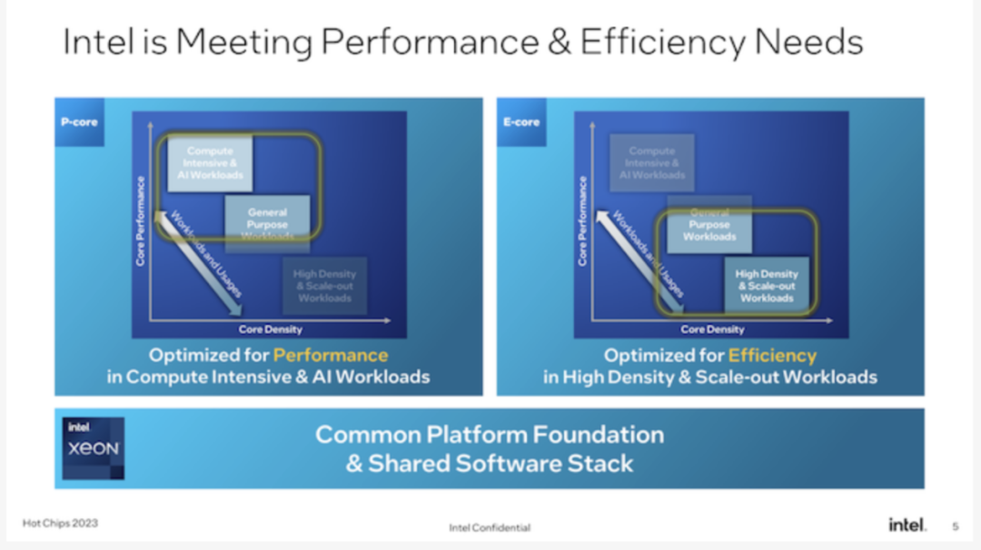
Since Intel plans to offer two distinct Xeons in one generation, an important factor in the sixth-generation Xeon scalable platform is that both processors will share the same platform. That means the same sockets, the same memory, the same chiplet-based design philosophy, the same firmware, etc. While there are still differences, especially when it comes to AVX-512 support, Intel is trying to make these chips as interchangeable as possible.
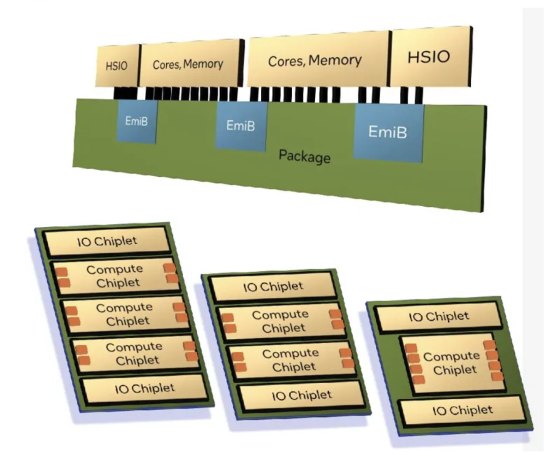
As Intel announced, both Granite and Sierra are chiplet-based designs, relying on a mix of compute and I/O chiplets that are stitched together using Intel's Active EMIB Bridge technology. While this isn't Intel's first dance with chiplets in the Xeon space (XCC Sapphire Rapids takes that honor), it's a unique evolution in chiplet design that uses a different compute/IO chiplet instead of combining Other "complete" Xeon chiplets are spliced together. Among other things, this means that Granite and Sierra can share a common I/O chiplet (built on the Intel 7 process), and from a manufacturing perspective, whether the Xeon is Granite or Sierra is "just" a question of which type of computing The chiplet has been put down.
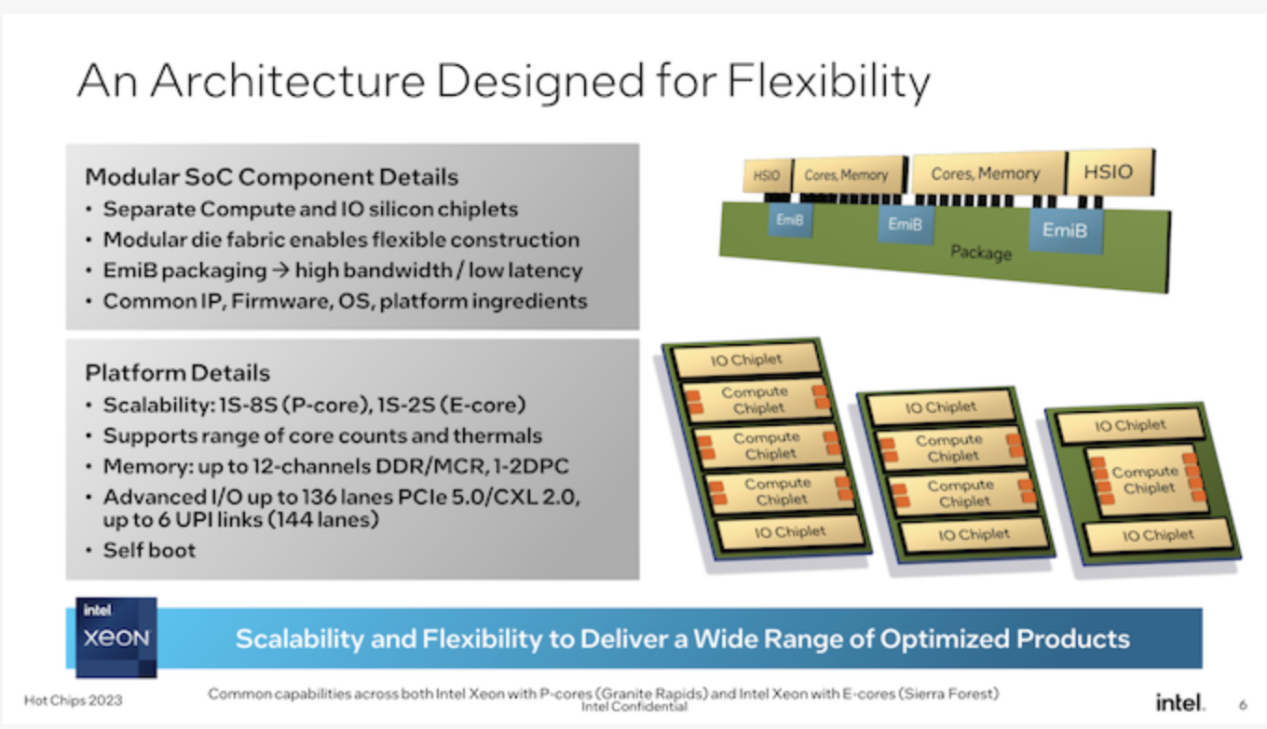
Notably, Intel has confirmed for the first time that the sixth-generation Xeon Scalable Platform is getting auto-boot capabilities, making it a true SoC. No external chipset (or FPGA) is required to operate these processors because Intel places all the necessary I/O functions required for operation within the I/O chiplet. This brings Intel's Xeon series closer in functionality to AMD's EPYC series, which has had similar auto-boot capabilities for some time.
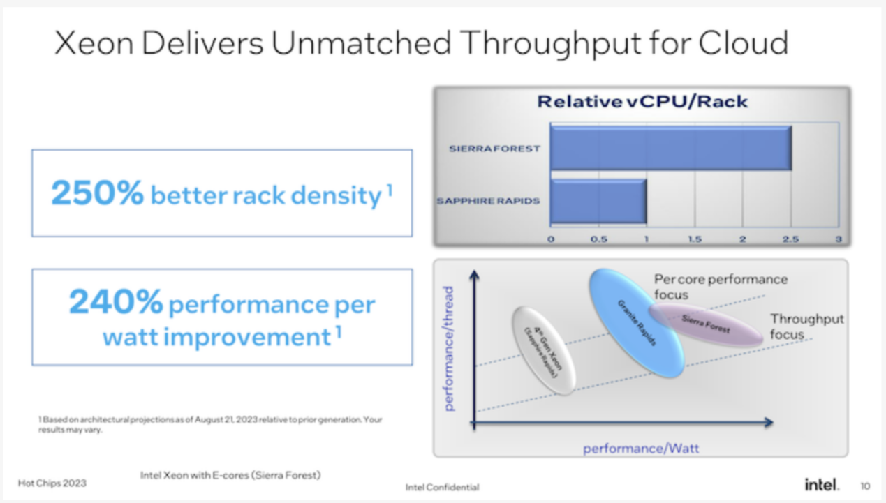
All told, the 6th generation Xeon scalable platform will support up to 12 memory channels and scale with the number and capabilities of existing computing chips. As Intel previously revealed, the platform will be the first to support new Multiplexer Combined Ranks (MCR) DIMMs, which essentially combine two groups/ranks of memory chips together , to double the effective bandwidth to and from the DIMM. Intel says that with higher memory bus speeds and more memory channels, the platform can deliver 2.8x more bandwidth than the current Sapphire Rapids Xeon.
As for I/O, the maxed-out Xeon will be able to offer up to 136 lanes of general-purpose I/O, as well as up to 6 UPI links (144 lanes total) for multi-slot connectivity. For I/O, the platform supports PCIe 5.0 (why not PCIe 6.0? The timing isn't right, we're told) as well as the newer CXL 2.0 standard. As is traditionally the case with Intel's big-core Xeons, the Granite Rapids chips will be able to scale up to a total of eight sockets. Sierra Forest, on the other hand, will only scale to 2 sockets due to the number of CPU cores in use and Intel's expectations for different use cases for its customers.
In addition to sharing platform details, Intel also provided for the first time a high-level overview of the architecture used by the E-core and P-core. As is the case with multiple generations of Xeon now, Intel is leveraging the same basic CPU architecture as its consumer parts. Thus, Granite and Sierra can be thought of as deconstructed Meteor Lake processors, with the Granite featuring Redwood Cove P cores and the Sierra featuring Crestmont E cores.
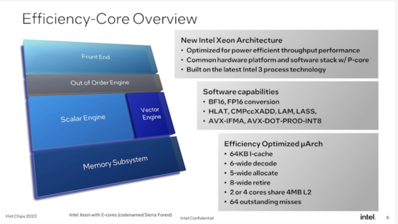
As mentioned, this is Intel's first attempt at offering E-cores for the Xeon market. For Intel, that means tuning its E-Core design for data center workloads, rather than the consumer-focused workloads that defined previous-generation E-Core designs.
While not digging into the architecture itself, Intel revealed that Crestmont is offering a 6-wide instruction decode pathway as well as an 8-wide retirement backend. While not as powerful as Intel's P cores, the E cores are by no means lightweight cores, and Intel's design decisions reflect that. Still, its design is much more efficient in die space and power than the P cores in Granite.
Crestmont's L1 instruction cache (I-cache) will be 64KB, twice the size of the I-cache in earlier designs. Intel rarely touches I-cache capacity (due to balancing hit rates and latency), so this is a notable change, and it will be interesting to see the ramifications once Intel talks more about the architecture.
Meanwhile, new members of the Crestmont E-core family can pack those cores into 2- or 4-core clusters, unlike Gracemont, which currently only offers 4-core clusters. This is essentially how Intel will adjust the ratio of L2 cache to CPU cores; no matter the configuration, the 2-core cluster has 4MB shared L2, and each core provides twice as much L2 for each core as it would otherwise. This essentially gives Intel another knob to tweak the chip's performance; customers who want a slightly more performant Sierra design (rather than just maxing out the CPU core count) can use fewer cores while getting a larger L2 cache resulting in higher performance.
Finally, for Sierra/Crestmont, the chip will provide instructions as close as possible to Granite Rapids. This means BF16 data type support, as well as support for various instruction sets such as AVX-IFMA and AVX-DOT-PROD-INT8. The only thing you won't find here, other than the AMX matrix engine, is support for AVX-512; Intel's ultrawide vector format isn't part of Crestmont's feature set. Eventually, AVX10 will help with that, but for now that's as close as Intel can get to parity between the two processors.
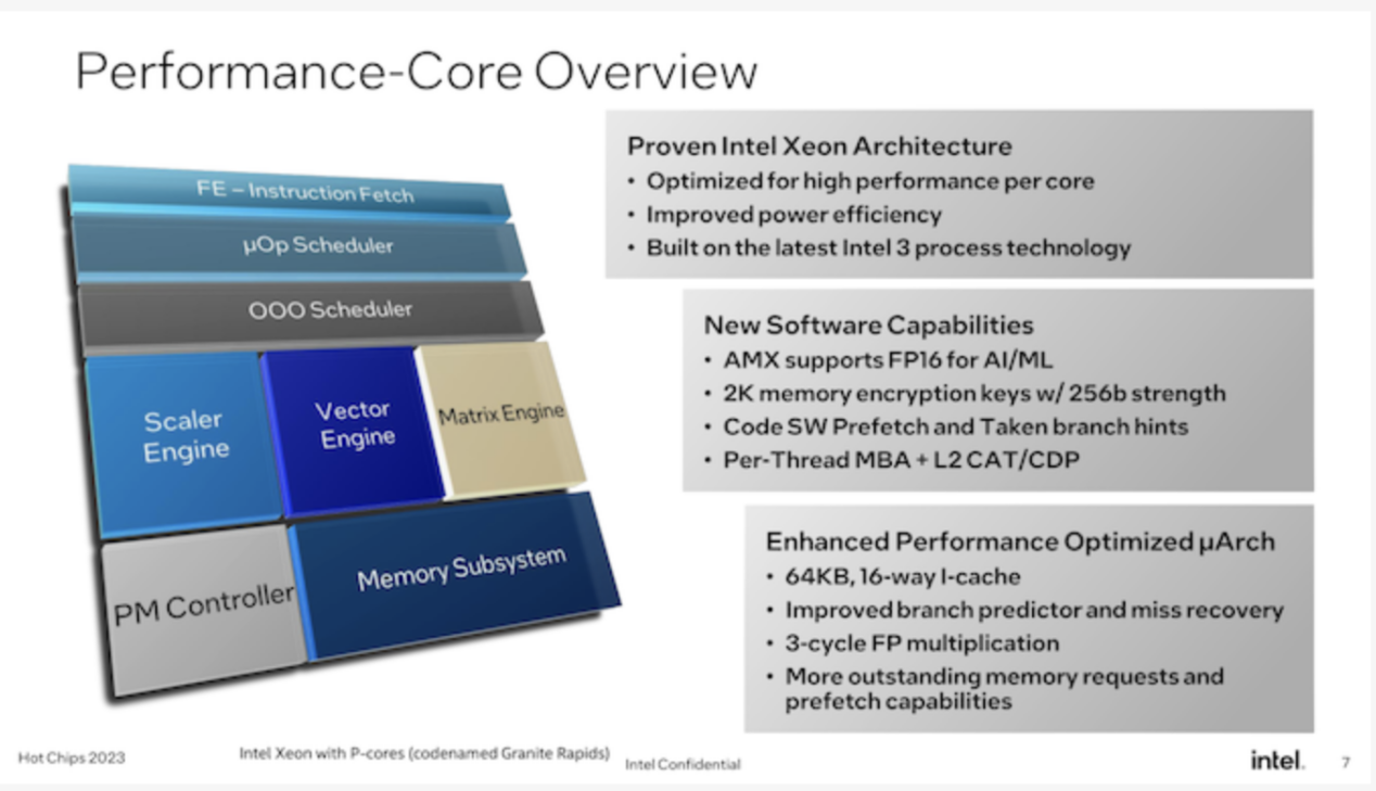
Meanwhile, for Granite Rapids, we have Redwood Cove P cores. Redwood/Granite is the traditional core of Xeon processors, and for Intel, the change is not as big as Sierra Forest. But that doesn't mean they stand by.
In terms of microarchitecture, Redwood Cove gets the same 64KB I-cache as Crestmont, twice the size of its predecessor. But most notably, Intel managed to further reduce the latency of floating-point multiplication, reducing it from 4/5 cycles to just 3 cycles. Basic instruction latency improvements like this are rare, so they're always welcome.
Other than that, the remaining highlights of the Redwood Cove microarchitecture are branch prediction and prefetching, typical optimization targets for Intel. Anything they can do to improve branch prediction (and reduce the cost of rare mistakes) will tend to pay relatively large dividends in terms of performance.
Redwood Cove's AMX matrix engine has received FP16 support, especially for the Xeon series. FP16 is not used as much as BF16 and INT8 which are already supported, but it improves the flexibility of AMX in general.
Memory encryption support is also being improved. The Redwood Cove version of Granite Rapids will support 2048 256-bit memory keys, while Sapphire Rapids supports 128 keys. There are also some enhancements to the Cache Allocation Technology (CAT) and Code and Data Priority (CDP) features, with Intel extending them to be able to control what goes into the L2 cache, rather than just the previous LLC/L3 cache implementation.
Ultimately, it goes without saying that Intel believes their upcoming Xeon processors will be ready in 2024 and beyond. By increasing the performance of the high-end P-core Xeons while introducing E-core Xeons for customers who just need a lot of lighter CPU cores, Intel believes they can address the needs of the entire market by sharing both CPU core types on a common platform.
While it's too early to talk about individual SKUs for Granite Rapids and Sierra Forest, Intel tells us that core counts are increasing overall. The Granite Rapids part will offer more CPU cores than the Sapphire Rapids (60 for the SPR XCC), and of course the Sierra's 144 cores will offer more CPU cores. It's worth noting, though, that Intel won't be splitting the two CPU families by core count -- Sierra Forest will also offer products with smaller core counts (unlike AMD's EPYC Zen4c Bergamo chips). This reflects the different performance capabilities of the P and E cores, and there's no doubt Intel wants to fully embrace the scalability that comes with using smaller chips.
While Sierra Forest already features 144 CPU cores, Intel also made an interesting comment in our pre-briefing that their first E-Core Xeon Scalable processor could have had a higher core count. But the company decided to prioritize per-core performance more, resulting in the chip and core numbers we'll see next year.
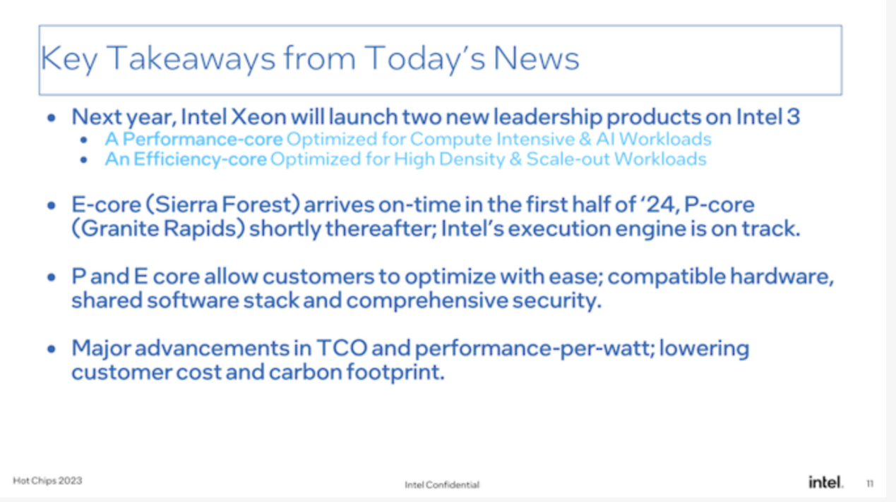
On top of that, Intel is emphasizing that their next-generation Xeon processors are still on track to launch in 2024, a fact that perhaps keeps marketing on Hot Chips a little too long. Needless to say, Intel is just recovering from massive delays in Sapphire Rapids (and the knock-on effects in Emerald Rapids), so the company is keen to reassure customers that Granite Rapids and Sierra Forest are where Intel's timing is back on track. Between previous Xeon delays and taking a long time to bring E-core Xeon scalable chips to market, Intel doesn't dominate the data center market like it once did, so Granite Rapids and Sierra Forest will mark an important An inflection point for the future development of Intel's data center products.
AMD Siena makes its debut
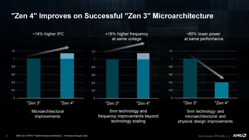
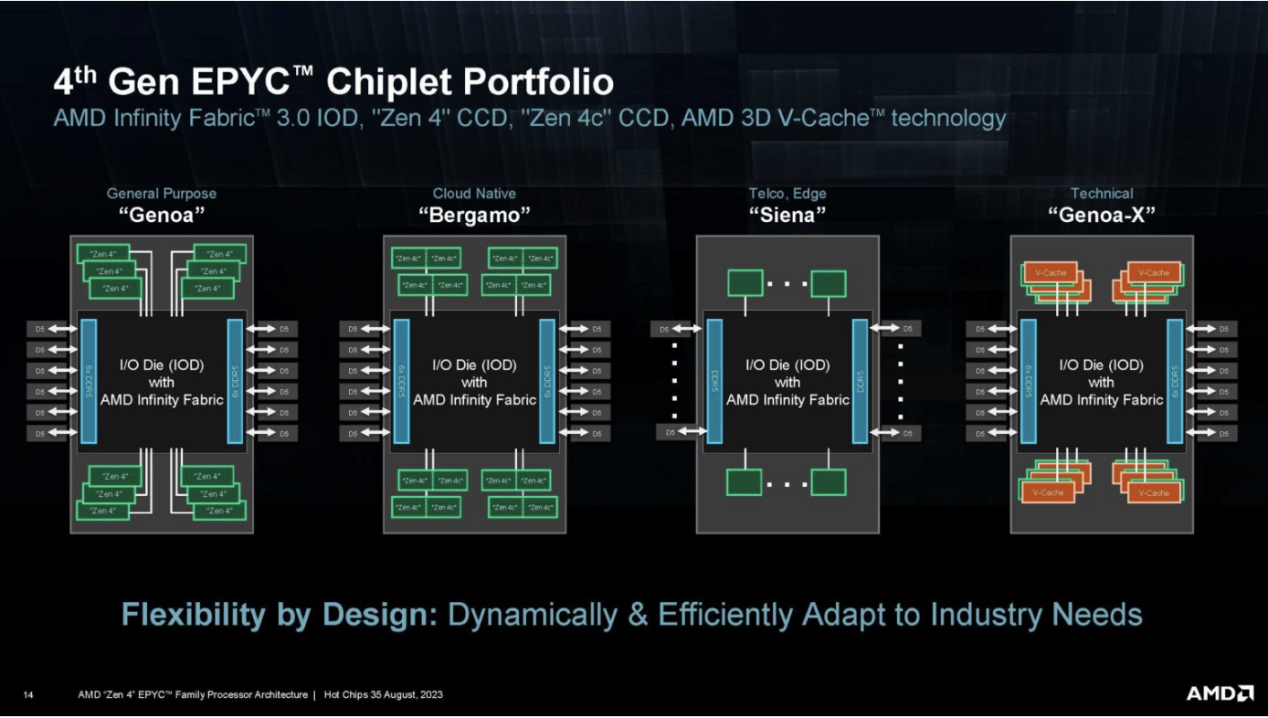
At Hot Chips 2023, AMD detailed the AMD EPYC Genoa, Genoa-X, and Bergamo CPUs. It also showcased key specifications of the upcoming Siena platform in the presentation.We know that AMD Zen 4 is a major upgrade over Zen 3 used in AMD EPYC 7003 "Milan", with higher IPC, more clocks, and lower power consumption.
Zen 4c brings a more compact Zen 4 core to Bergamo. Even so, AMD is still focused on making large CPUs. On Hot Chips, they showed a low-end solution.
AMD's Socket SP5 strategy is to build different chiplets and combine them with general-purpose I/O chips.
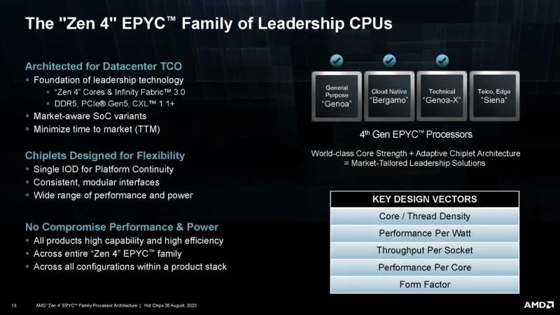
Now, AMD is showing off the fourth member of its 4th generation AMD EPYC portfolio, Siena for the telecom edge market.
 So far, we have disclosed the most about Genoa. We only have a maximum of 64 cores and 6 DDR5 DRAM channels. The scale of Siena will be much lower than Genoa, with a TDP of 70W to 225W, although not as low as some of Intel's Xeon D components.
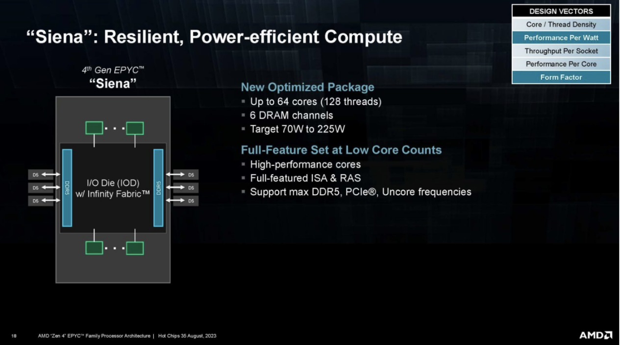 AMD requires lower power components because Intel has its single-chip Sapphire Rapids component, which is very attractive for cores up to 32 cores and is the main sales segment in the market. The 96 or 128 core 350W+is great, but they are not suitable for applications that require CPUs below 150W.
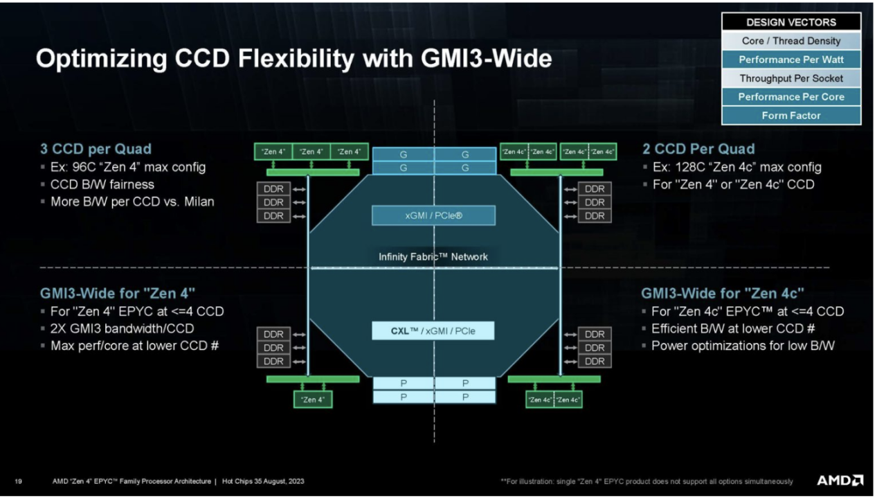
AMD also presented an interesting CCD slide showing some of the functions of the I/O chip.
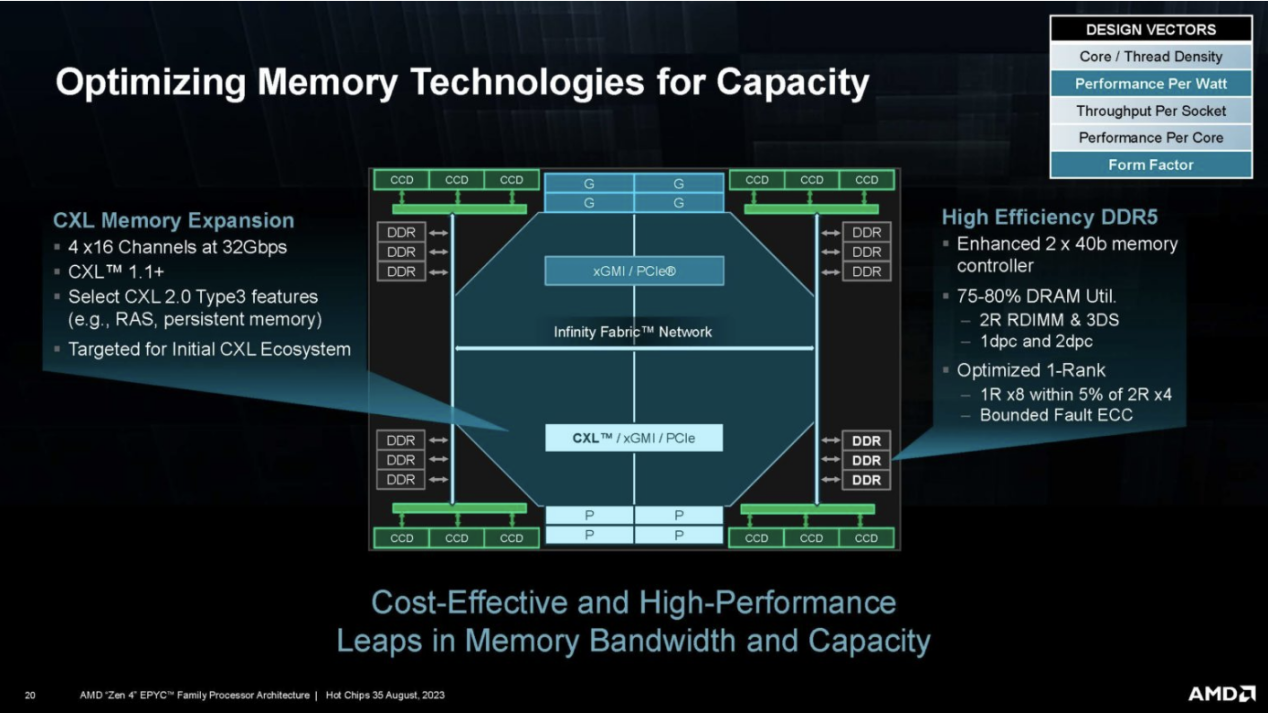
 This is a great slide. AMD also has a memory technology, including CXL.
 We're very excited about the launch of AMD EPYC Siena because AMD has a big hole in its server portfolio in the low-power space. We finally see how AMD can achieve this with half the DDR5 channels and fewer cores.
Arm brings two processors
At this year’s hotchips, Arm brought more sharing of Arm Neoverse V2 and Neoverse N2.Arm Neoverse V2 is part of the current generation of Neoverse solutions. Arm is committed to providing the reference core for the data center and infrastructure markets. Neoverse V2 is more of a high-performance data center CPU core, while N2 is more of an infrastructure.
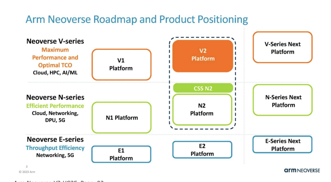
We have previously introduced Neoverse V2, which aims to improve the performance of Neoverse V1 designs used by companies such as AWS in the Graviton series.
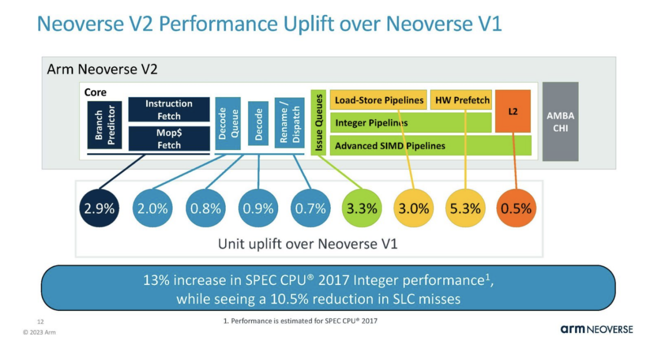
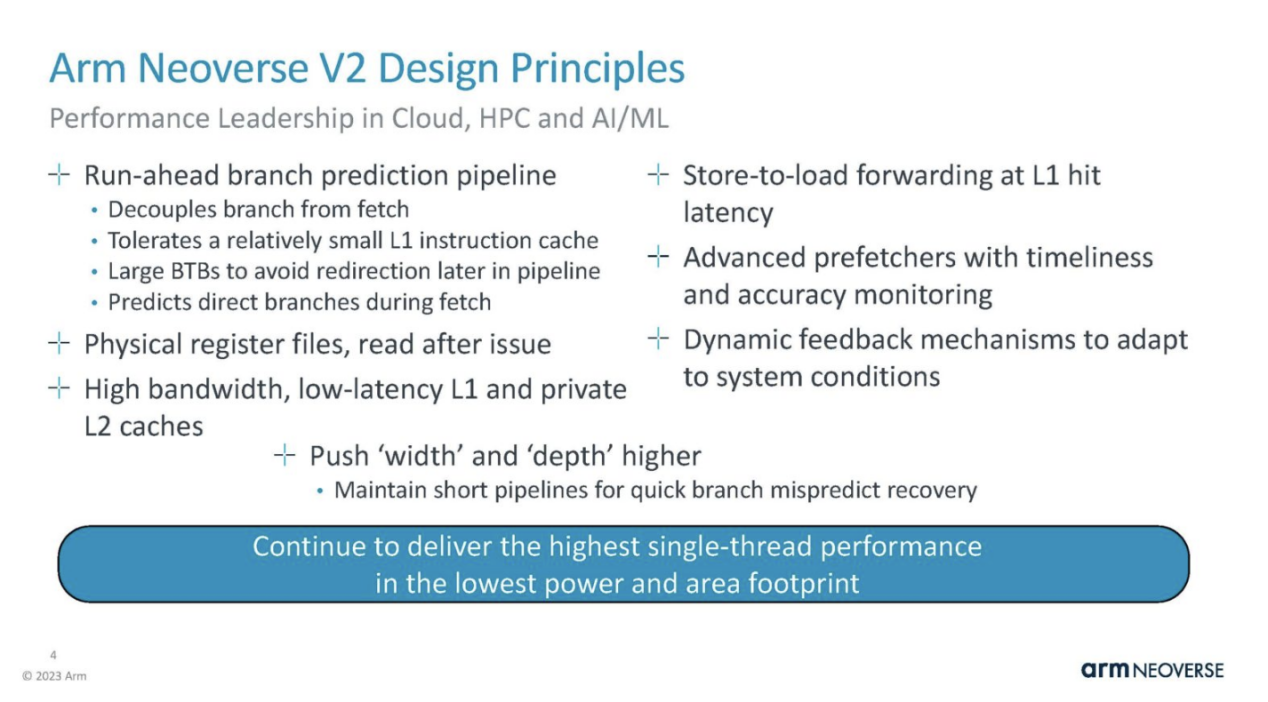 Arm Neoverse V2 is the Armv9 architecture. Here is a chart showing the highlights of the core section.

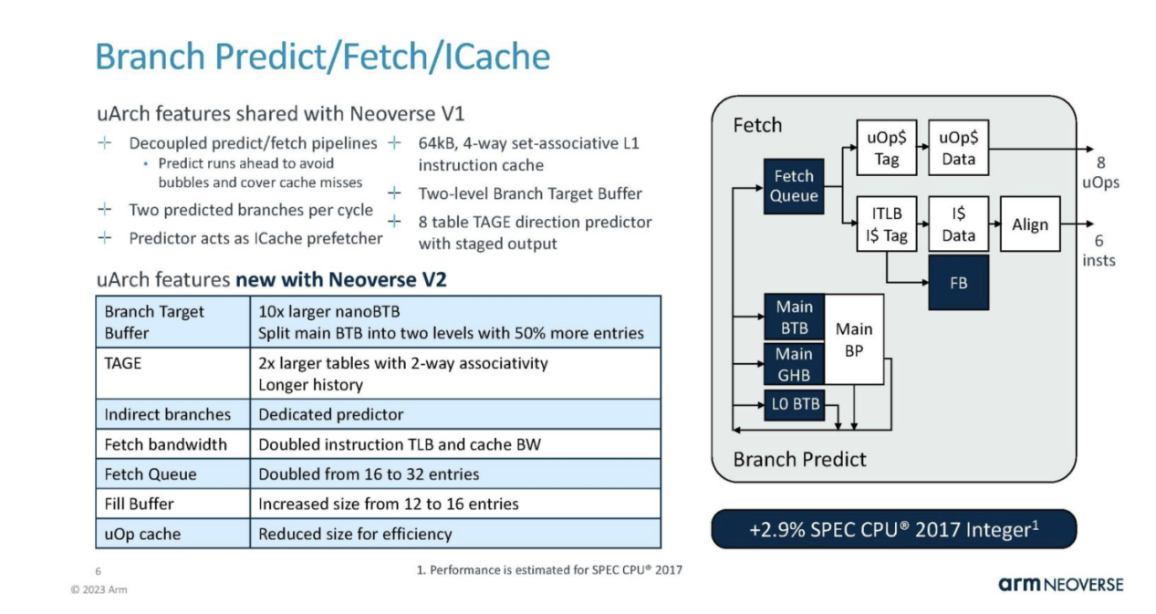
On the branch, predict/fetch/ICache is partially shared with Neoverse V1, but with some major improvements. It's pretty cool that Arm shows the performance impact of these changes in each section.
 This is the theme for V2. It is mainly based on V1 to continuously upgrade and provide more resources.
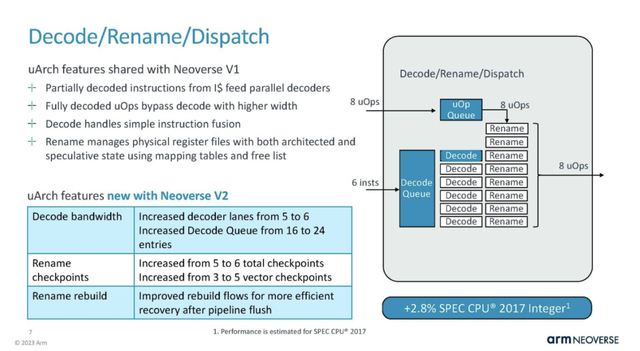
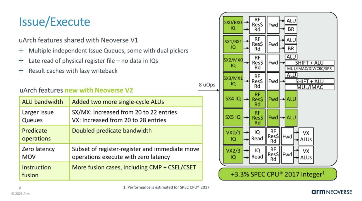
The issue/execution aspect is a significant change in V2.
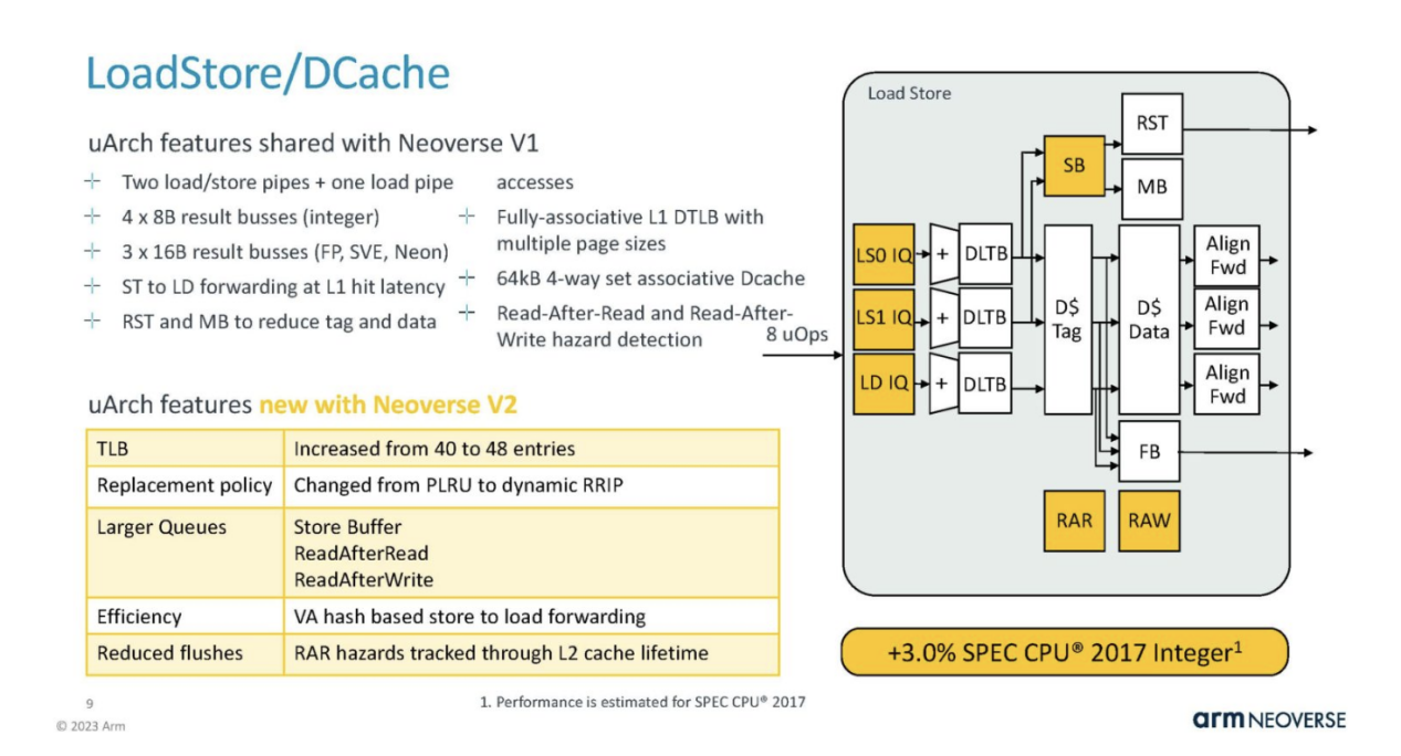
 Load/Store and DCache have undergone changes, such as a 20% increase in TLB.
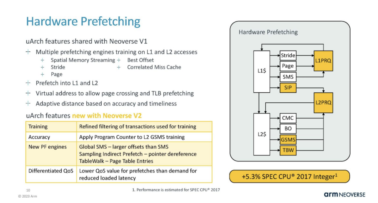
This also means that Arm needs to improve the hardware prefetching of the kernel to keep the execution units and cache running.
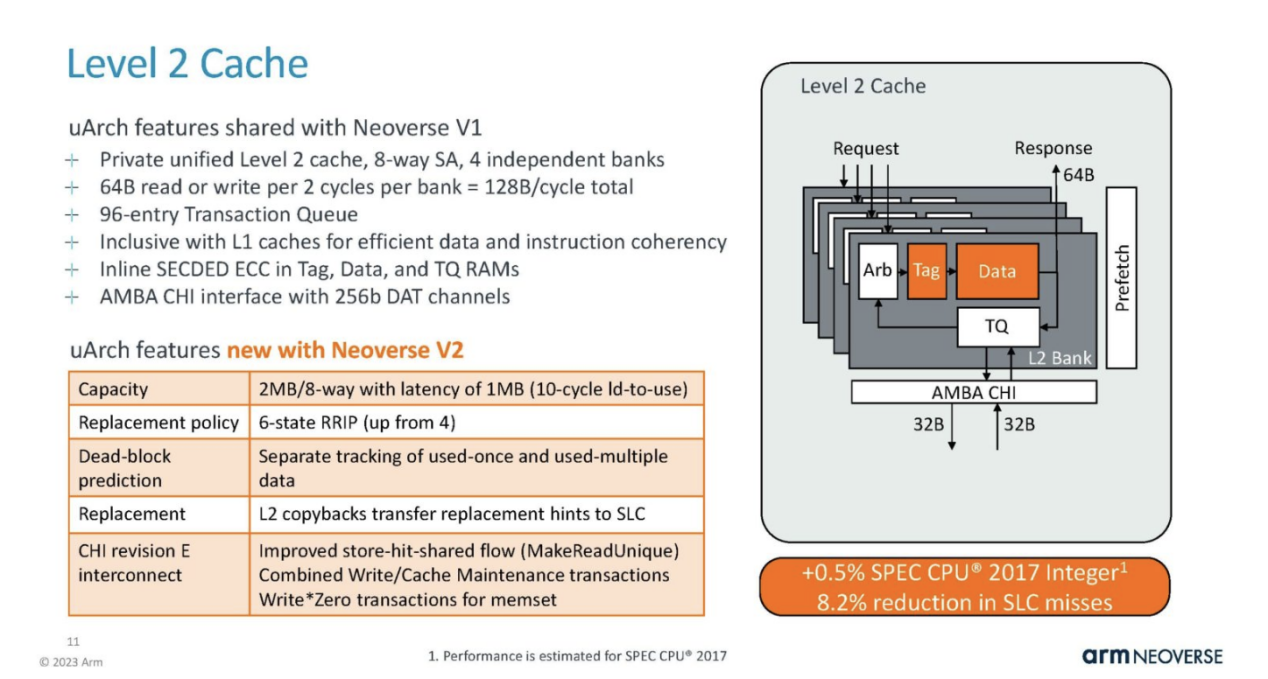
 L2 caching is private to each core and an important feature of the data center. This is a smaller SPEC Int gain region.
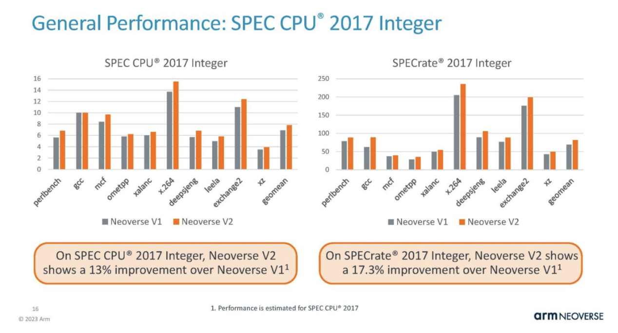
Arm stated that compared to V1, these V2 changes combined resulted in a performance improvement of approximately 13% for each kernel. If added, the number for each section does not equal a 13% increase. This is because some changes can affect others, so the total is less than the sum of each individual improvement area.
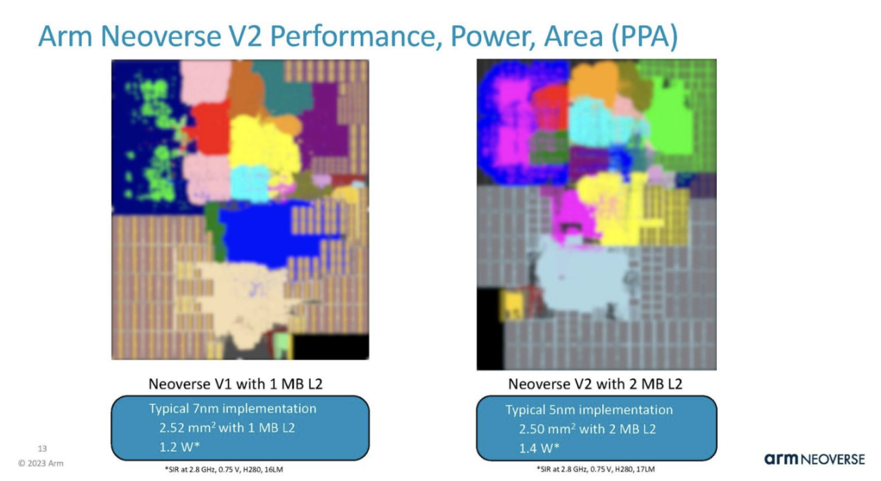
 Arm stated that the new core has shrunk from 7 nanometers at TSMC to 5 nanometers. Although the L2 cache has doubled, the power consumption has only increased by about 17% and the area is roughly the same. Interestingly, the Arm in the above slide indicates that V2 is 13% faster, but the following slide uses 16.666% power.
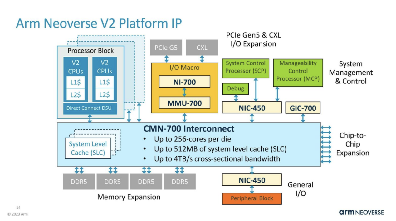
 In addition to the V2 kernel itself, the platform also has functions such as CMN-700 interconnection, which can provide more cache and increase the number of cores. For the Arm Neoverse core, this is the core, not the entire chip, so it is necessary to purchase items such as PCIe Gen5 IP.
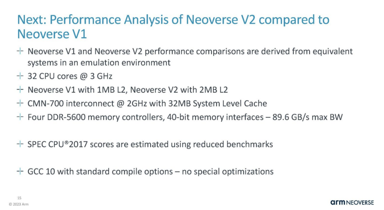
 The following are the assumptions for performance results:
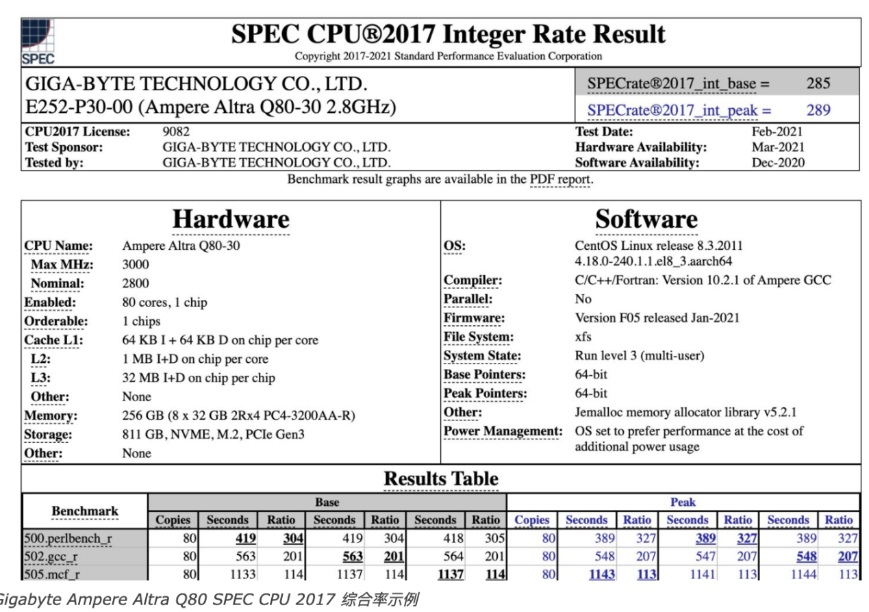
 Arm is demonstrating its integer performance. During the pre briefing conference call, the analyst inquired about the difference between the two estimated results, as the chart on the right is labeled "SPECrate", but neither is labeled as base or peak. Arm cannot confirm this. Our best guess is that the left image is the base image and the right image is the peak image, but this is just a guess because Arm cannot confirm what they are displaying.
 These results are only estimates, but the following are the actual submitted results, where the results are labeled with baseline and peak values. Surprisingly, CPU companies are unable to answer this question.