In the past 30 years, the market share of Japan's semiconductor industry has dropped from more than 50% to 10%, but the market share of semiconductor equipment manufacturers has always maintained a 30% market share and has remained extremely competitive.
Metrans is verified distributor by manufacture and have more than 30000 kinds of electronic components in stock, we guarantee that we are sale only New and Original!
In 2022, four Japanese companies ranked among the top 10 semiconductor equipment manufacturers by sales. The four companies are: Tokyo Electronics (TEL) ranked fourth, Advantest ranked sixth, Screen ranked seventh, and Kokusai Electric ranked ninth, followed by Hitachi High-Tech, Nikon, Canon and other companies back.It is precisely because of these equipment manufacturers that the Japanese media and government have the confidence to make the bold statement that "without Japanese-made semiconductor equipment, semiconductors will not be manufactured."
Front-end supremacy
In the semiconductor production process, the "front-end process" refers to the process of etching circuits on a silicon wafer to make a chip. The manufacturing process will vary slightly depending on different products such as logic semiconductors and storage semiconductors, but approximately 700 processes are required from the front-end process to the finished chip.
There are the following processes in the semiconductor manufacturing process: "exposure" and "development" (i.e., sintering circuit patterns on the wafer through a photomask), "etching (removing unnecessary films according to the circuit pattern)", forming metal "Film formation" of wiring and insulating films, "diffusion" of injecting ions into the wafer to make it a semiconductor, "planarization (CMP, Chemical Mechanical Polishing)" of flattening metal films and insulating films, "Cleaning (cleaning the residue on the wafer surface between each process)", and each process needs to be repeated dozens of times.
Then, the wafer is cut into chips and enters the back-end process. Each process requires extremely high technical strength, and Japanese companies have obvious advantages in each process.
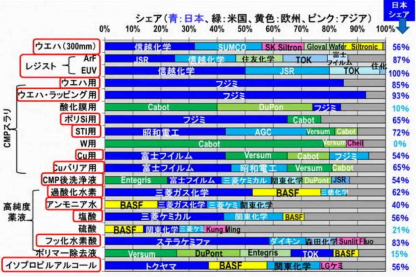
The figure below shows the share of the main manufacturing equipment used by Japanese companies in the front-end process. The largest shares are photoresist coating and development equipment (92%) and heat treatment equipment (also called vertical diffusion furnace) (93%). , chip cleaning equipment (63%) and batch cleaning equipment (86%), and length-measuring electron microscopes (CD-SEM) (80%). Apart from this, CMP devices do not have a high share, but EBARA has a large share (about 30%) of logic semiconductors, so it is also counted as a device with a high share.

On the other hand, although Japan has a low share of exposure equipment, dry etching equipment, CVD, sputtering and other thin film deposition equipment, and various inspection equipment, these equipment also use many Japanese-made parts and equipment, of which absolutely Most quartz and ceramic components are made in Japan.
More importantly, Japan is also far ahead in the share of the main materials used by various companies for pretreatment. Materials with a high market share in Japan include silicon wafers, various resists, various CMP slurries, various High-purity chemicals, etc. It can even be said that Japanese material manufacturers have a stronger presence than equipment manufacturers.
The reason why Japanese semiconductor equipment manufacturers have maintained their international competitiveness for a long time is undoubtedly that Japanese companies have maintained long-term trade relations and established close cooperative relationships with global advanced semiconductor manufacturers.
Every time a semiconductor is updated to a new generation, its R&D expenses will increase accordingly. As R&D partners of semiconductor manufacturers, equipment manufacturers are extremely important in the process of advanced miniaturization by learning miniaturization technology and improving their own value. Therefore, among the leading Japanese semiconductor equipment manufacturers in the world in terms of sales, their overseas customers’ sales contribution rate reaches more than 80%.
Japanese characteristic business management
Since Japanese semiconductor equipment manufacturers began to expand their business very early, they were hardly affected by the decline of Japanese semiconductors.
There were once some manufacturers known as "Japanese comprehensive motor manufacturers", but now they have almost disappeared from the world market. Most Japanese semiconductor manufacturers are just a subsidiary division of a comprehensive motor manufacturer, while most equipment manufacturers have maintained a high degree of independence and self-operation to achieve their current status.
But this is just one of the symptoms. First of all, companies with a high market share in Japan usually deal with liquids, fluids and powders, which have no fixed initial shape and are "fluffy". Therefore, they are very complex and have many parameters that need to be optimized. In this case, the Japanese find the best solution through experience and intuition. This process requires a large amount of tacit knowledge and know-how, which cannot be artificialized and can only form a skilled technology or craft.
In such a world, continuous improvement and perfection in the workshop is the key to success. Some Japanese media stated that the serious and patient Japanese will optimize even the smallest details. Therefore, equipment, materials and components are all produced from the bottom up. came out, these Japanese characteristics have become the source of high market share.
On the other hand, four European and American companies, Applied Materials (AMAT), Lam Research (Lam), KLA and ASML, have higher market shares in industries with lower market shares in Japan. They generally go through the market first. Marketing determines needs. Then, scientific research is conducted at the beginning of the development of various types of equipment. Based on these needs and science, the entire facility is designed from the top down by a strong leader. In this process, equipment tends to be modular.
In addition, simulation technology is used at every stage of the device development process. In addition, technology and know-how are converted into software and incorporated into equipment, which are then integrated into a single world-standard equipment.
Japanese media said that the behavior of European and American equipment companies seems to reflect the rigid contract society of Europe and the United States, which has also led to Japanese equipment manufacturers usually customizing equipment for each customer semiconductor manufacturer, while Western equipment manufacturers basically only develop one global standard equipment.
If we dig deeper, the differences in concepts and behaviors between Japanese and European and American people are the main reasons for these differences.
Japanese media believe that Europe and the United States generally have theories first. Then, in the early stages of development, conduct full discussions and unify policies. Then, standards, rules, stories and logic are formulated. On the other hand, European and American engineers are not good at doing experiments, but leave experiments to a profession called technicians.
Japanese technicians, on the other hand, rely on their superior senses and experience to conduct experiments intuitively with their hands. They are very good at optimizing within an established framework, but are not good at formulating standards and rules, which ultimately leads to a high or low share of equipment and other products.
Specifically, compared with Europe and the United States, Japanese equipment manufacturers have obvious advantages in the film-forming series of processes. For example, Tokyo Electronics, Japan's largest company, has a very high market share in coating & developing (Coater/Developer) equipment, while SCREEN has a high market share in cleaning equipment.
In addition, Japan also has many excellent chemical manufacturers that can provide photosensitive materials (Resist), various medical solutions, ultrapure water and other chemicals. These manufacturers all have high market shares and also provide strong support for equipment. factory.
In addition, most equipment manufacturers use Japanese yen as the trading unit, so their performance is rarely affected by the exchange rate.
In today's semiconductor industry, there is a saying that "the process has advanced to 3 nanometers and is about to approach the physical limit." Therefore, related companies are improving semiconductor performance by using technologies other than miniaturization. Its most advantageous complementary technologies are "Chiplet" and "advanced packaging".
The backend cannot be underestimated
The so-called "Chiplet" refers to making each component of the chip separately, such as Core, storage, etc., and connecting them electrically to design the functions of a single chip, while "new generation packaging" refers to the original ones arranged side by side. The chips on the substrate are 3D vertically stacked, or highly integrated "Chiplet", and packaged on the substrate.
To realize "Chiplet", a new generation of packaging technology, it is necessary to use technical elements related to packaging and testing of the semiconductor back-end process. In fact, not only in the field of back-end equipment, Japanese substrates, substrate materials, back-end materials and back-end equipment A mutually reinforcing relationship has already been formed.
While Japan’s share of copper-clad laminates for low-end general-purpose printed circuit boards (PCBs) is negligible and dominated by Chinese and Taiwanese manufacturers, Japan’s share of copper-clad laminates for high-end packaging exceeds 65% %, and has reached a 100% monopoly in terms of packaging build-up substrates and packaging solder resists.
In addition, among the packaging substrate manufacturers, Japan's IBIDEN and Shinko Electric play an indispensable and unique role in the field of server processors.
In the market for post-processing materials. Japan's lead frame share remains at 37%, and its market share in molds used as sealing materials exceeds 65%. In addition, Japan monopolizes 88% of the molding materials for FOWLP (fan-out wafer-level packaging), such as InFO (integrated fan-out WLP) developed by TSMC for Apple iPhone, and Japan’s share of underfill materials has also reached 92%, close to to the point of monopoly.
In the specific back-end equipment market, Japan monopolizes 90% of the dicing machine market. Although the placement machine market share is only 10%, the molding market share reaches 65%, and the test market share reaches 55%. More than half of them were.
Japanese companies have a very high presence in back-end equipment. For example, DISCO's wafer cutting equipment (Dicer, which cuts wafers into chips) has a very high market share in the world. After the chip is packaged on the substrate, it will be molded with epoxy resin, and TOWA has a high influence in the molding process. In addition, Sumitomo Bakelite's plastic resin has a very high market share. In the semiconductor back-end process, Japanese material manufacturers have unparalleled technical strength in specific fields.
It is worth mentioning that in recent years, in order to further effectively leverage the advantages of Japanese companies in the back-end processes, many overseas companies have entered Japan. For example, TSMC established a R&D base in Tsukuba City, Ibaraki Prefecture, Japan in June 2022, and Samsung Electronics invested 30 billion yen in Yokohama City to set up a R&D base and put into test production lines. The above-mentioned bases are all related to back-end processes.
With the development of generative AI, more and more semiconductors will require "chiplet" and new generation packaging technology, so this has become a driving force for semiconductor manufacturers to accelerate research and development. The performance of some equipment manufacturers has begun to reflect orders related to back-end processes. Orders for Tokyo Electronics' "Wafer Bonder (wafer bonding equipment, mainly used for high-density packaging to bond wafers together)" equipment are rising. It is reported that sales in 2023 are expected to reach tens of billions of yen.
It is reported that thanks to the impact of the growth in demand for advanced packaging related to generative AI, DSICO has also received relevant financing and will begin to contribute to performance growth from October to December 2023 at the earliest.
It is predicted that the demand for equipment and materials related to "Chiplet" and advanced packaging will further increase in the future. If equipment related to the process can be developed and put into practical use as soon as possible, it will bring new growth opportunities to Japanese companies.
Uncertainties
However, the development of Japanese equipment manufacturers is definitely not smooth sailing. Although it has maintained a high market share for many years, its market share has not increased. Although part of the reason is due to exchange rate factors, under the current trend of depreciation of the yen, the market share has dropped to 30%, which is less than the 40% or even higher that year.
The main reasons are as follows. The expensive EUV lithography machine is dominated by ASML of the Netherlands. The first market share of etching equipment that is comparable in scale to exposure equipment has been taken by Lam Research of the United States. In addition, Japan has not won the emerging markets in recent years. ALD (atomic layer deposition) equipment market. Some people believe that in the emerging semiconductor equipment field, only American manufacturers have an advantage.
In addition, China's equipment manufacturers are also growing rapidly. According to Japanese media reports, as of 2021, there are five Chinese companies among the top 30 global semiconductor equipment manufacturers in terms of sales. China's Northern Huachuang has sales of 8.43 billion yuan in the first half of 2023 (January-June). Compared with the same period last year, it increased by 55%.
As the industry says, "Investment is the best way to cultivate equipment manufacturers." The government's supportive policies encourage semiconductor manufacturers to continue to invest in equipment. In the future, Chinese equipment manufacturers will enter the "equipment localization" stage, which will further Affect the future performance of Japanese equipment manufacturers.
Where are the opportunities?
The situation of regional equipment share shows that since 2012, Japan's market share of semiconductor equipment has declined sharply, and by 2022 it has dropped to less than half of the US market share, only 24%.
After analysis, it can be found that the market share of almost all equipment has been declining in the past 10 years. Some practitioners said that under such circumstances, it is difficult to say that "Japanese manufacturing equipment is very powerful." Moreover, if market share continues to decline, it will be difficult for Japan to continue supplying equipment to the world. The current situation is very dangerous. If action is not taken now, Japan's equipment industry may follow the same path as the semiconductor memory industry.
A company's "competitiveness" refers to the company's ability for individual products or product lines to satisfy existing customers and attract purchases from potential customers. According to this definition, if a company becomes more competitive, its sales share will not decline. In terms of growth rate, it should not be inferior to its competitors either. However, the growth rates of many Japanese front-end equipment manufacturers are lower than their counterparts in Europe, the United States and South Korea. This means that the competitiveness of Japanese front-end equipment manufacturers is declining.
Japanese media stated that the era of "Japan's front-end equipment power" is becoming a thing of the past, and if Japanese semiconductor equipment manufacturers want to maintain and increase their market share in the future, they can only cooperate with cutting-edge semiconductor manufacturers to develop cutting-edge processes. In the research and development of cutting-edge semiconductor fields, we cannot relax even for a moment.
The semiconductor production equipment market size in 2022 is 14 trillion yen (approximately RMB 700 billion). It is predicted that by 2030, the semiconductor market size is expected to reach 100 trillion yen (approximately RMB 5 trillion). Correspondingly, the equipment market size It is expected to be close to 20 trillion yen (approximately RMB 1 trillion).
Today, it is difficult for the world to see large-scale acquisitions (M&A) and business integration cases like in the past. If Japanese equipment manufacturers want to continue to exert their advantages on the international stage, they can only defeat their competitors in cutting-edge fields.